

|
|
1.INTRODUCTIONExtreme ultraviolet lithography (EUVL) is the most promising next generation lithography technique for sub-16 nm node and below. EUVL has been in development for about a quarter century and is now getting ready for high-volume manufacturing (HVM) of semiconductor devices expected to start in 2015. However, there are still many uncertainties for the success EUVL even though ASML’s first production tools are ready to use.1 The EUVL pilot lines to test whole process in manufacturing sites are largely ready but productivity and unknown cost of defect mitigation and mask infrastructure remain challenges for the HVM phase. There is still an unsettled EUV source power performance gap that must be solved. Defect qualification, inspection, and review processes are key issues of mask fabrication in both blank and patterned masks.2, 3 Defect-free masks are a crucial issue for EUVL in HVM, however manufacturing masks without defects seems unfeasible, because reflective EUV masks are vulnerable to defects created during deposition process of blank mask and handling. Therefore, achieving EUV masks with the lowest defect density with an acceptable yield is targeted. EUV blank mask defects have been reduced to a minimum level that can be applied to memory chips, but further improvements are needed to meet the requirements of logic devices.4 There are many successful efforts to repair defects at patterned EUV mask in case of minimum defect density, but the native defects in the blank, such as phase defects, are particularly problematic since they are not repairable. To use the masks that have native defects with the lowest density, fiducial marks can be used for mask alignment if the phase defects on the masks are located accurately.5 Therefore, EUV mask inspection and review tools are necessary to locate the defects with a sustainable yield, minimize the printable defect numbers to a production level, and classify the quality of defects to lithographic printability. Review processes to classify all printable defects are mandatory before defect cleaning, mitigation, and avoiding process using fiducial marks. The development of a sensitive actinic imaging tool is essential to evaluate the impact of defects due to the wavelength-specific response of defects and large penetration depth into the Mo/Si multilayer optics at EUV wavelength.6 In order to characterize the effects of the internal phase defects, there are many efforts to develop EUV actinic inspection and review tools.6, 7 There are several successful mask review tools that have been developed, e.g., Fresnel zone plate imaging,3 full reflective aerial image measurement tool,2 and coherent scattering microscopy (CSM).8 The traditional actinic review systems using optics (i.e. Fresnel zone plates and reflective projection optics) have several limitations such as optics aberrations, tight alignment tolerances, a low transmission throughput of the optical components, high cost of highresolution EUV optics, and sensitivity to vibrations. Moreover, the phase information, which is very elusive and critical for EUV masks, can be obtained either indirectly or through focus scans. In addition, the coherent scattering microscopy is limited to specific purpose of critical dimension (CD) metrology of periodic patterns. In this report we present a lensless EUV actinic mask review tool, which is based on scanning coherent diffraction imaging (CDI) method, i.e. ptychography.9, 10 In this technique, diffracted light from the sample is measured while the sample is scanned across a coherent illumination. Redundant scattering information from the sample is collected by overlapping the illumination in neighboring scan positions. The image of the sample is reconstructed via iterative computational calculations to a resolution much smaller than the illuminating beam size. Ptychography provides both amplitude and phase information. It has been demonstrated in a wide range of wavelengths from visible light to hard X-rays, as well as for electron microscopy11. With the development of effective reconstruction algorithms, ptychography has become rather a routine technique in advanced microscopy where either optics is difficult to manufacture or phase information is of interest. To test actinic EUV mask imaging using by ptychography we developed a ‘Reflective EUV Mask Scanning Lensless Imaging’ (RESCAN) prototype, which has been recently installed at the XIL-II beamline of the Swiss Light Source (SLS), Paul Scherrer Institute, Switzerland. We show the first imaging performance of this tool through reconstructed aerial images of a resolution test pattern on a multilayer mask using 0.1 (0.4/4) NA and nontelecentric (6° of angle) illumination. We discuss its potential for actinic mask inspection in various cases, such as line and space (L/S) dense patterns, isolated patterns, as well as phase defects. 2.THEORETICAL BACKGROUND: PTYCHOGRAPHIC IMAGINGCDI provides a phase image without the need for optical components for detection. For CDI, the diffracted intensity distribution has to be Nyquist sampled and the illumination should be coherent. In principle, the high scattering wave-vectors available in the Fraunhofer diffraction plane can produce wavelength-limited resolution. There have been several efforts to develop actinic EUV mask imaging tools using coherent diffraction imaging. EUV coherent scattering microscopy (CSM that is also known as CDI) has been demonstrated to measure 88 nm half-pitch (hp), (i.e., for hp 22nm node, 1X) and below on EUV masks13, and it provides lithographic properties8, 14 (e.g., MEEF, H-V CD bias, NILS etc.). CSM is an effective tool for CD metrology, nevertheless it is limited to periodic patterns and relatively insensitive to isolated and small native defects in blank masks. Ptychography is a scanning variant of CDI that provides high-resolution imaging with both amplitude and phase information of the specimens without the need of high-NA illumination or imaging optics. Ptychography relies on collecting a series of diffraction patterns, from mutually overlapping scan positions, as shown in Figure 1(a). The measured intensity of each neighboring diffraction pattern from overlapping scan positions provides information that allows retrieval of the diffraction pattern phase through iterative reconstruction algorithms.9 Figure 1.Illustration of ptychographic imaging. (a) The specimen is scanned with a compact illumination, represented here by white circles, such that there is sufficient overlap between neighboring positions. (b) For each illumination position a coherent diffraction pattern is recorded. (c) The reconstructed phase image of the test specimen.  From the initial estimates of the illumination (i.e., “probe” P) and the specimen (i.e., “object” O) and from the measured diffraction patterns the iterative algorithm calculates an exit wave (Ψ) for a particular sample position.9 where r is a vector in the plane perpendicular to the optical axis on the sample, rj is relative shift between the sample and the illumination function. In the extended ptychographical iterative engine (ePIE) reconstruction algorithm12 the difference between the exit wave from the initial wave is used to make an update of the estimated value of the object (O) and illumination (P). In our experiments, the sample is scanned through the beam with a step size about five to ten times smaller than the beam diameter. At each step a far-field diffraction pattern is collected on a pixel detector as shown in Figure 2(b). For ptychography the conditions of the illumination are relaxed because it does not require a priori characterization or detailed knowledge of the illumination probe, and the beam size should be small enough in order to measure the far-field intensity patterns by a CCD detector. The complex-valued transmissivity (or reflectivity in our case) of the sample can be reconstructed via iterative transform algorithms. The advantage of ptychography, compared to lens-based imaging, is that resolution is not limited by optics. In contrast to other kind of lensless imaging (e.g., holographic techniques15), it requires no reference beam because the data arising from overlapped beam positions introduces redundancy and robustness on the reconstruction.16 For ptychography the measurement is preferentially conducted with high spatial coherence. This coherence and size requirements are relatively relaxed and easy to achieve. Ptychography has been demonstrated and it is rapidly developing as a versatile microscopy tool for various applications.15, 17 Figure 1 shows a schematic of data acquisition and processing for ptychography. 3.REFLECTIVE EUV MASK SCANNING LENSLESS IMAGING TOOL (RESCAN)Our prototype tool for actinic mask inspection using ptychography, RESCAN has been installed at the XIL-II beamline with undulator source is extendable from EUV to BEUV wavelength due to the tunability of the light source and optics. RESCAN consists of a condenser of Fresnel zone plate (FZP), sample stage and CCD detector. It is constructed as a flexible tool where the incidence angle, wavelength, bandwidth, and numerical aperture, can be varied in a simple manner. As a system based on ptychography, RESCAN offers many advantages for actinic imaging of EUV masks. First, resolution is not limited by imaging optics or a given spot size. Secondly, it provides both amplitude and phase information of the specimen simultaneously whereas conventional microscopes need through-focus scans for the reconstruction of high contrast phase images,18 which allows to characterize defects Third, it is very flexible to change the illumination conditions such as incidence angle and wavelength. RESCAN is designed for imaging of blank and patterned EUV masks, with periodic, non-periodic or isolated patterns, at EUV wavelength and 6 degrees of incidence angle, and therefore fully emulating the imaging conditions of EUV scanners. To aid in our system design, we simulated data acquisition and reconstruction using the extended ptychographical iterative engine12. The XIL-II beamline is designed for EUV interference lithography19, which enables high-resolution aerial images down to 7 nm hp. The source is an undulator providing spatially coherent EUV light with 13.5 nm wavelength, 4% bandwidth and about 30 mW power. The source power is far above the requirements of RESCAN. To obtain temporal and spatial coherence in the illumination we designed the illumination optics that simultaneously monochromatize the beam and generate a small spot size on the sample using a combination of FZP and pinhole. The experimental geometry for reflection mode actinic mask review system using ptychography is shown in Figure 2, which consists of a FZP, an order sorting aperture (OSA), a reflective multilayer mirror, and a pinhole. EUV light (13.5nm wavelength) was illuminated on the sample surface with 6° incidence angle, and a CCD detector, with a sample to detector distance range between 80 mm and 120 mm, used to measure diffraction patterns. The FZP has 1000 μm diameter and a focal length of 150 mm at 13.5 nm wavelength, and is used in combination with a 60 μm OSA. In order to produce a coherent EUV spot we use a Ni pinhole of 5 μm diameter that is manufactured by e-beam lithography on a 100 nm thick silicon nitride Si3N4 membrane. The window of 300 μm diameter square was made on the same membrane to measure diffraction. Downstream of the focusing optics we use a reflective multilayer mirror (MLM which was coated by Optixfab) to direct the EUV beam on to the sample surface. The sample is 500 μm downstream from the pinhole and is exposed to the focused coherent EUV beam with a 6 degree off-axis illumination and with a spot size of 10 μm at the object plane. A soft x-ray CCD detector (Princeton Instruments, PI-SX: 1340×1300) is used for data acquisition. Schematic design of RESCAN is presented in Figure 3. This system is designed to be very flexible so that we can change the illumination angle from 4 to 10 degrees, numerical aperture from 0.06 (0.24/4) to 0.12 (0.48/4), and wavelength from 6.5 nm to 13.5 nm. The beam spot size on the sample can be set in the range of 5 μm to 30 μm depending on the wavelength and experimental configuration. For scanning of the sample with high precision, necessary for high-resolution imaging with ptychography, a three-axis piezo stage (nPoint: NPXY100Z100-series) was used with two horizontal and one vertical axis. All three axes have piezoelectric actuators and a capacitive measurement system. We measured less than 10% repeatability error with 10 nm steps on the capacitive sensor and less than 1% linearity error in the total range of 100 μm. Figure 3.Schematic design of the RESCAN system. (a) The mechanical and optical components in the RESCAN chamber consisting of flexible 3D-FZP stage, OSA, ML mirror and micro membrane holder on the 3D-piezo sample stage. (b) Schematic design of RESCAN system with a CCD detector on top. 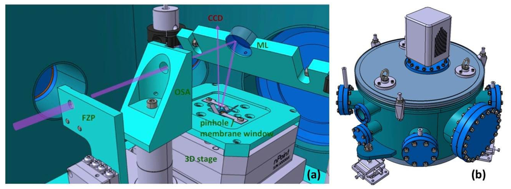 All the components of the RESCAN were designed, manufactured at PSI, except for the piezoelectric-stage and multilayer mirrors. The FZPs, micro membrane unit and test patterns on multilayer substrates were fabricated in the Laboratory for Micro- and Nanotechnology (LMN) in PSI. The RESCAN system was installed at the XIL-II beamline (X09LB) in December 2014. Figure 4 shows the two chambers at XIL beamline where interference lithography and mask review tool are installed. Figure 4.Photo of the XIL-II beamline in February 2014. EUV interference lithography system and Reflective actinic EUV mask review system are installed on the optical table in clean-room environment.  Figure 5 shows the first ptychography measurements measured with RESCAN performed on a resolution test pattern that consisted of 50 nm-thick nickel absorber patterns on a Mo/Si multilayer substrate. These patterns were fabricated using e-beam lithography at LMN of PSI. A scanning electron microscope (SEM) image of this sample, which consists of squares and L-patterns with 400 nm feature size, are shown in Figure 5(a). Two measurements were performed where sample was scanned with step sizes of 1 μm and 400 nm, through a beam of approximately 10 μm in diameter. Figure 5(b) shows a typical diffraction pattern captured with the CCD during the experiments on this sample. The ePIE algorithm was adapted to the reflective EUV conditions and a starting guess for the probe was calculated by simulating a focused beam 500 μm downstream of the focus, which is the approximate distance to the pattern. As mentioned in previous sections, ptychography enables the simultaneous reconstruction of the probe, i.e. the incident beam, which is shown in Figure 5(c). For the ptychography measurements with a 1 μm step size, some artifacts in the reconstructed image is observed, as shown in Figure 5(d). A reconstruction of high fidelity and high-resolution is obtained with a 400 nm step size between positions, as shown in Figure 5(e). In this reconstructed image, the obtained resolution is estimated to be about 100 nm, using 10%-90% edge response of the squares and L-patterns. These results are preliminary and further measurements and detailed analysis will be the subjects of future reports. Figure 5.Imaging results obtained with RESCAN. (a) SEM image of structures on a multilayer EUV reflecting sample. The squares and L-shapes are with 400 nm feature size. (b) Reconstructed illumination incident on the sample. (c) Diffraction pattern measured with the CCD detector, shown here with saturation in order to visualize details of the speckle pattern. Reconstructed images for scans with (d) 1 μm step size and (e) 0.4 μm step size  4.SUMMARY AND OUTLOOKWe have developed a new method of EUV actinic mask inspection method by using ptychography in reflection. Advantages of this lensless imaging technique include that it provides both amplitude and phase information of the specimen with high resolution and potentially high throughput. RESCAN has been recently installed at the XIL-II beamline of the SLS. Its imaging performance with 0.1 (0.4/4) NA, 6° of angle of incidence off-axis illumination, is demonstrated here using a test pattern on which we obtained well-resolved images of patterns with 400 nm feature size. Preliminary experiments yielded a resolution of 100 nm. We note that the system is designed for 80 nm resolution (i.e. 20 nm after mask demagnification on wafer) and we will perform further experiments in order to achieve this resolution. In addition, we would like to study the effect of different parameters, such as bandwidth, spot size and step size, on the resolution and sensitivity. Future plans involve improving the tool towards 20 nm resolution (5 nm on wafer) and a capability of scanning full size EUV masks. This work shows the potential of ptychographic methods for high-resolution imaging in EUV and soft X-ray range. We present our prototype RESCAN and show that ptychography is a very promising approach for high-resolution and high-throughput reviewing of EUV masks. We believe that the RESCAN can substantially contribute to the studies on mask defect identification and repair. With the development of stand-alone coherent EUV sources and further development of this method, ptychography can be a powerful method for the realization of actinic mask inspection tools with high resolution and throughput. ACKNOWLEDGEMENTSWe are grateful to XIL-II team members, group members of LMN and technical teams of SLS for their technical assistance and constructive discussions. The EUV measurements were performed at the XIL-II beamline, Swiss Light Source (SLS), Paul Scherrer Institute, Switzerland. REFERENCESHendrickx, E., Gronheid, R., Hermans, J., Lorusso, G., Foubert, P., Pollentier, I., Goethals, A., Jonckheere, R., Vandenberghe, G., Ronse, G.,
“Readiness of EUV Lithography for Insertion into Manufacturing: The IMEC EUV Program,”
Journal of Photopolymer Science and Technology, 26 587
–593
(2013). https://doi.org/10.2494/photopolymer.26.587 Google Scholar
Uzzel, D., Garetto, A., Magnusson, K., Tabbone, G.,
in Proc. of SPIE,
(2013). Google Scholar
Goldberg, K. A., Mochi, I., Benk, M., Allezy, A. P., Dickinson, M. R., Cork, C. W., Zehm, D., Macdougall, J. B., Anderson, E., Salmassi, F., Chao, W. L., Vytla, V. K., Gullikson, E. M., DePonte, J. C., Jones, M. S. G., Camp, D. V., Gamsby, J. F., Ghiorso, W. B., Huang, H., Cork, W., Martin, E., Every, E. V., Acome, E., Milanovic, V., Delano, R., Naulleau, P. P., Rekawa, S. B.,
in Proc. SPIE,
(2013). Google Scholar
Wurm, S.,
“EUV lithography readiness: ConFab presentation preview,”
Solid state technology,
(2012) http://electroiq.com/blog/2012/05/euv-lithography-readiness-confab-preview/ Google Scholar
Huh, S., Kearney, P., Wurm, S., Goodwin, F., Han, H., Goldberg, K., Mochi, I., Gullikson, E., , “EUV Actinic Defect Inspection and Defect Printability at the Sub-32 run Half-pitch,” LBNL Paper LBNL-2714E, (03-30-2010) (2010). Google Scholar Mochi, I., Goldberg, K. A., La Fontaine, B., Tchikoulaeva, A., Holfeld, C.,
in Proc. of SPIE,
(2010). Google Scholar
Goldberg, K., Mochi, I.,
“Wavelength-Specific Reflections: A Decade of EUV Mask Inspection Research,”
International Workshop on EUV Lithography,
(2009). Google Scholar
Lee, S., Doh, J. G., Lee, J. U., Lee, I., Jeong, C. Y., Lee, D G., Rah, S., Ahn, J.,
“Carbon contamination of EUV mask and its effect on CD performance,”
Current Applied Physics, 11 S107
–S110
(2011). https://doi.org/10.1016/j.cap.2011.07.019 Google Scholar
Rodenburg, J. M., Hurst, A. C., Cullis, A. G., Dobson, B. R., Pfeiffer, F., Bunk, O., David, C., Jefimovs, K., Johnson, I.,
“Hard-X-Ray Lensless Imaging of Extended Objects,”
PRL, 98
(2007). https://doi.org/10.1103/PhysRevLett.98.034801 Google Scholar
Thibault, P., Dierolf, M., Menzel, A., Bunk, O., David, C., Pfeiffer, F.,
“High-Resolution Scanning X-ray Diffraction Microscopy,”
Science, 18 379
–382
(2008). https://doi.org/10.1126/science.1158573 Google Scholar
Humphry, M. J., Kraus, B., Hurst, A. C., Maiden, A. M., Rodenburg, J. M.,
“Ptychographic electron microscopy using high-angle dark-field scattering for sub-nanometre resolution imaging,”
Nature Communications, 3 730
(2012). https://doi.org/10.1038/ncomms1733 Google Scholar
Maiden, A. M., Rodenburg, J. M.,
“An improved ptychographical phase retrieval algorithm for diffractive imaging,”
Ultramicroscopy, 109 1256
–1262
(2009). https://doi.org/10.1016/j.ultramic.2009.05.012 Google Scholar
Harada, T., Nakasuji, M., Nagata, Y., Watanabe, T., Kinoshita, H.,
“Phase Imaging of Extreme-Ultraviolet Mask Using Coherent Extreme-Ultraviolet Scatterometry Microscope,”
Japanese Journal of Applied Physics, 52
(06GB02),
(2013). Google Scholar
Doh, J., Jeong, C.Y., Lee, S., Lee, J. U., Cha, H., Ahn, J.,
“Determination of the CD Performance and Carbon Contamination of an EUV Mask by Using a Coherent Scattering Microscopy/In-situ Contamination System,”
Journal of the Korean Physical Society, 57 1486
–1489
(2010). https://doi.org/10.3938/jkps.57.1486 Google Scholar
Eisebitt, S., Luning, J., Schlotter, W. F., Lorgen, M., Hellwig, O., Eberhardt, W., Stohr, J.,
“Lensless imaging of magnetic nanostructures by X-ray spectro-holography,”
Nature, 432 885
–888
(2004). https://doi.org/10.1038/nature03139 Google Scholar
Guizar-Sicairos, M., Fienup, J. R.,
“Phase retrieval with transverse translation diversity: a nonlinear optimization approach,”
Optics Express, 16 7264
–7278
(2008). https://doi.org/10.1364/OE.16.007264 Google Scholar
Holler, M., Diaz, A., Guizar-Sicairos, M., Karvinen, P., Färm, E., Härkönen, E., Ritala, M., Menzel, A., Raabe, J., Bunk, O.,
“X-ray ptychographic computed tomography at 16 nm isotropic 3D resolution,”
Scientific Reports
(2014). Google Scholar
Diaz, A., Trtik, P., Guizar-Sicairos, M., Menzel, A., Thibault, P., Bunk, O.,
“Quantitative x-ray phase nanotomography,”
Phys. Rev. B, 85
(020104),
(2012). Google Scholar
Ekinci, Y.,
“Extreme UV interference lithography: progress and prospects,”
SPIE newsroom,
(2013) https://spie.org/x95096.xml Google Scholar
|


