|
|
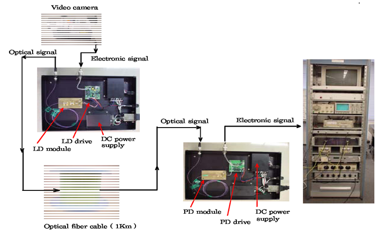
1.IntroductionOptical fiber technology [1] is becoming the key technology of advanced telecommunications, optical measurements and sensing and so on in a variety of fields. In order to study the optical fiber telecommunications system the students have to learn about the theory of transmitting laser light in fiber and some optical properties related with laser light. Recently, we have introduced the new technical training about the basics of optical transmitting system for the students of Department of Information Systems Engineering at our university [2], [3]. The system mainly consists of two basic optical modules and two electronic drives for them. One of the two is the laser diode module which converts electronic signal into optical intensity signal and mainly uses a laser diode (LD) as a light source. The other is the photodiode module which converts the transmitted light signal into the electronic signal again and mainly uses a photodiode (PD). In these modules, the main important and essential technologies to be trained are fabrication technique with an accuracy of few micrometers according to the size of fiber core and also assembling technique for electronic analogue drive circuits. Through the training, students fabricated the laser diode and photodiode modules at the starting stage and then measured the characteristics of both modules. After that they assembled the LD and PD drive circuits and measured some characteristics of both drives. Lastly, they tested the fabricated modules and the assembled drives by checking the transmitted image using an optical fiber cable. In the present paper, the contents of the training are described from a view point of student technical training from which they can learn about not only the basics of optical transmission technology, but also some practical assembling techniques with an accuracy of only a few micrometers and how the optical telecommunication technology is supported by precision machinery and electronic technologies. 2.Training scheduleThe training is planed for one semester for junior students at the Department of Information Systems Engineering. It has 6 steps which consists of the module fabrications of LD and PD modules, the measurements of the characteristics of both modules, the basic training of an operational amplifier (op amp), the assembling of LD and PD drive circuits, the measurements of characteristics of LD and PD drive circuits, the rough estimation of signal and noise ratio in transmitted image signal using the LD and PD modules and optical fiber cable, and so on. The schedule of the training is shown in Fig. 1. In each step the training times are denoted and one unit of time is 6 hours including the times for explanation to students about training subjects. 3.Optical Fiber Transmission Practice SystemThe whole optical fiber transmission practice system is shown in Fig. 2 which consists of a video camera, LD(λ =1.5 µm), PD modules and their drives, optical fiber cable and some electronic instruments. To understand the electronic circuit of drives in the modules, students have to study and understand about the fundamental functions and workings of op amp through the practices of the circuits, such as an inverting amplifier, a noninverting amplifier, a differential amplifier, an integrator circuit and so on. Then they assemble the circuits of the drives. The technical training has been done as described in the following sections. 4.Laser Diode and Photo Diode Modules4-1Laser diode moduleThe assembled LD module was shown in Fig. 3 and was connected to the LD drive circuit as shown in Fig. 4 to send the modified signal of laser light to the PD module which is placed lKm away from the LD module. Fig. 3.A photograph of the assembled laser diode module. Figure 4. Laser diode (LD) module and its drive circuit.  The assembling components of the modules shown in Fig. 5 consists of these parts; (a) a brass base plate of 40mm × 80mm square, (b) a laser diode, (c) a holder plate, (d) the attached laser diode to the holder plate, and (e) a lens holder, the first lens attaching to the laser diode and a plate with screws. Fig. 5.Components of the laser diode module, (a) a brass base plate(40mm × 80mm), (b) a laser diode, (c)a holder plate, (d) the attached laser diode to the holder plate and (e) a lens holder, the first lens attaching to the laser diode and a plate with screws  The laser diode used here is OL5300N (Oki Electronics) which emits the wavelength of 1.5 µ m and 10mW. The diode is fixed to the plate of which the size is 40 mm and 80mm and 5mm in thickness with a screw. The first lens of which the diameter is 5mm and 10 mm in length and is used to convergence the laser light into the core of a fiber cable of which the diameter is 10 µ m. The diode was fixed to the plate temporally and the electric lead wires were connected to the electrodes of the diode as shown in Fig 6(a) to check the emitted laser light using a constant current power supply (Oyokouken YN54AD), a light power meter (Anritsu ML9001A), and an infrared sensor plate(Q32R, International Inc) for detecting and seeing the laser light by eye shown in Fig. 6(b). Here, the spatial distributions of the light intensity emitted from the laser diode were measured in the horizontal and vertical directions as shown in Fig. 7 at the distance of 75mm between the laser diode and the photodiode for measuring the intensity of laser light at the injection current of 20mA. The emitted laser light shows almost same spatial intensity distribution in both directions. Fig. 6.(a) the laser diode attached to the plate and a power meter, (b) an infrared sensor plate for detecting the light from the laser diode.  Fig. 7.Measurement result of spatial distribution of the light intensity emitted from the laser light.  After checking the laser emission from the diode, the base plate and the LD were placed on a assembling jig as shown in Fig. 8(a). Fig. 8.(a) the first lens connected to the laser diode is adjusted, (b) fixing the first lens by an instant adhesive agent.  Next, an isolator, of which size is 5mm in diameter and 10.5mm in length as shown in Fig. 9(a), was also fixed at 5mm a way from the diode holder as shown in Fig. 9(c). In a fixing procedure, the special attention was needed to set the isolator in correct direction of it. In the case of its right direction, the output laser beam becomes one, but it becomes two beams in the case of wrong direction. The isolator was adjusted and fixed as to the output beam is coincident with the optical axis of the laser diode by using a manipulator and two wedge plates of which the size is 8mm × 12mm and 3mm in thickness as shown in Fig. 9(b). The second lens was also attached at 6mm from the end of the first lens and connected to an end of the fiber cable. The lens holder was wiped up with ethanol and then the lens and the fiber were set on an attachment of the manipulator. Then, the laser light,0.63 µ m in wavelength, of He-Ne entered into the fiber cable at the other end of the cable having a FC connector to adjust coarsely the optical axis of the second lens by using a corner cube. The FC connector was taken off from the He-Ne laser and connected to the power meter. The current power supply was switched on and the current of 20mA was injected to the laser diode, then adjustment of the optical axis of the second lens was carried out prudently with spending much time moving the x and y axes of the manipulator, thus inclining the assembling stage and reading the output of the power meter and lastly the lens was fixed at the most appropriate position. Fig. 9.(a) an isolator of which the diameter is 5mm and 10.5mm in length, (b) wedge plates to fix the isolator as shown in (c). 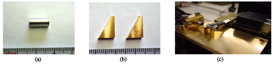 The laser light passed through the LD holder, the isolator, the second lens and then the fiber cable. After adjusting the position of the second lens, the two wedge plates were arrayed to fix the lens. At this moment special attention must be paid to array the two plates to be put in the same direction to keep the adjusted optical axis. The two wedge plates were fixed temporarily by using the instant adhesive agent as checking no change of the readings of the power meter. A final fixing was done by using another adhesive agent (Semedaine Hi-super 5 A and 5B) as shown in Fig. 10. The characteristic of the injection current and the output laser power in the assembled LD module was measured as shown in Fig. 11. The power was about 1.1mW at the current of 20mA. 4-2.Photodiode ModuleThe PD module was also assembled as shown in Fig. 12(a) and (b) in this training which is used in the system, In a similar way of the LD module, the PD module was assembled using some components such as a photodiode (OD8121N), a holder and a base plate. First the photodiode was fixed on its holder and placed on the base plate. Then a lens was connected to a ferrule of the fiber and fixed in front of a photodiode window. A He-Ne laser was used to set the position of the lens appropriately. The laser beam of the He-Ne entering from the FC connector of the fiber cable passed through the lens and entered the photodiode. The output current of the photodiode was measured to check the detection for the incident laser light by an electronic multi meter. After checking the current, the fiber was connected to another laser light source of 1.5 µ m in wavelength, which is the same wavelength used in the module and then the lens was adjusted accurately by using the light power meter and a light attenuator shown in Fig. 13. After doing the final adjustment, the two wedge plates were also used here to fix the lens on the plate by using the same adhesive agent which is used for the LD module. Some of the characteristics of the PD module were measured in the training. The relationship between the input light power of laser light and the output current of the photodiode was obtained as shown in Fig. 14. The output current is almost linearly proportional to the input power. Fig. 14.Measurement result of input light power of the laser and the output current of the photodiode.  The ratio of the output current and the input laser power at the wave length rage from 1460nm to 1570nm were obtained as shown in Fig. 15. The ratio, which shows the conversion efficiency of input power of the laser light into the current (A/V) ranged from 0.6 to 0.8 that is approximately close to an ordinal value of 1.0. That means that the assembled PD module was considerably good quality. 5.Laser Diode Drive CircuitThe LD drive circuit assembled in this training is shown in Fig. 16 and also the photographs of electronic components, a board for assembling and the assembled circuit are shown in Fig. 17. The circuit was assembled on the board which is prepared for this circuit and the symbols of electronic components used in the circuit are printed on it so that students could put each device on the board correctly by doing the check of the values of it and the polarity of capacitors and by watching the position in the circuit. It is seemed to easy to assemble the electronic devices on the board, however soldering the electrodes of IC chips of op amps or wires in small space with sure electric contact and fully electric isolation with neighbor ones are sometimes difficult. Students felt difficulties because the space gap between the electrodes to be soldered is about 0.7mm. Through the work for soldering them, they could notice its importance. Fig. 17.Photographs of (a) electronic components, (b) assembling board of 50mm × 50mm square and (c) assembled LD drive circuit.  After assembling the circuit, the circuit was divided into two parts, 1) the constant current supply circuit to the laser diode, 2) the modulation circuit of electronic voltage signal to the intensity signal of the laser light, In each circuit the characteristics were measured as described below. The constant current drive circuit of laser diode is taken out as shown in Fig. 18 to measure the main characteristics of the circuit. Fig. 18.Constant current drive circuit. The relationships between the voltage Vo and the current Io, and also between the load resistance RL and Io were measured.  5.1The characteristic of zener diode.A zener diode is used in this circuit to generate constant voltage which make any level of voltage with a variable resistant to flow the current to the laser diode, In order to test the constant voltage of the zener diode, the current against the applied voltage was measured and obtained as shown in Fig. 19. The constant voltage of –2.5V was obtained as the zener voltage and any voltage between 0V and –2.5V could be set with the variable resistance. 5.2The characteristic of the set voltage Vo and the current Io of the laser diodeThe current to the laser diode is set at any level with the variable resistance in Fig. 18 which is connected parallel to the zener diode and the set voltage determines the controlling constant current Io to the laser diode. To control the current constant, the integrator circuit was used here in the usual way. Here, the explanation how to control the current if the load resistance of the laser diode changes with some reasons such as temperature changes. It is important to let the students understand the combination operation of the monitor voltage Vm of the current Io using a differential amplifier and integrator circuit. One example of the explanation was done using the figure 18 in which the current Io, the set voltage Vo, the monitor voltage Vm, which is the potential difference at the electric resistance Rm for monitoring the flowing currents and becomes the input voltage of the integrator, and the output voltage Vi of the integrator are drawn graphically against time. When the switch turns on at the time to, the output voltage Vi of the integrator is zero and immediately begins to decrease linearly with (ΔV/RC) · t, where ΔV = (−Vm + Vo) and Vo, Vm are negative voltage and also Vm=0 at to, t is time, R and C are the resistance and the capacitance of the integrator. It causes an increase in the current Io of the order of milli-ampere through the transistor. The increase in the current also causes an increase of Vm so that the input voltage Δ V of the integrator decreases and brings the rising speed of the current Io more slowly. When the time reaches at any time t1 and then Vm equals to Vo, the current Io becomes constant and can keep its value. Next, if the current changes slightly, say such as Io+ΔI, in that case Vm will immediately increase by ΔVm which is caused by increased ΔI and the output voltage Vi of the integrator will begin to increase with (Δ Vm/RC) · t from the constant voltage. This slight increase of ΔVm causes a small decrease in the current and when the current goes down to Io, Δ V becomes zero again that means that the current Io goes back to the initial set values. In the case of opposite change, the similar movement is done to keep always Io constant. The characteristic of the set voltage Vo and the current Io was measured as shown in Fig. 20. The current is linearly proportional to the set voltage and the rate of current and voltage was 105 mA/V. 5.3The stability of the current Io for electric resistance loadsAs described previously the current Io is influenced remarkably by a change in the electric resistance load. Here, the stability for load changes was tested under some values of the electric resistance replaced in the circuit instead of load changes of the laser diode used. The current Io was measured at the values of 5 Ω 、 10 Ω 、 15 Ω and 20 Ω as shown in Fig. 21. In the figure it is clearly seen that the current Io keeps constant values against the load and the changes of the current in this range was about 5% which shows that the circuit will work well as a constant current supply. 5.4The modulation characteristics of the electronic voltage signal to the current signalNext, the modulation characteristics were measured. The signal modulation is a very important function that converts the electronic voltage signal into the current signal that means the intensity of laser light to be transmitted in optical fiber cable. The modulation circuit is shown in Fig. 22 and consists of a differential amplifier added to the constant current supply circuit. The electric resistance of 10 Ω was put in the circuit instead of the laser diode. The electronic voltage signal to be converted into the current is input into the positive input terminal of the amplifier. On the other hand any polarity voltage can be input into the negative input terminal in order to add the biased voltage to the modulation signal. The biased voltage Vb was set at zero. Here, the modulation currents of Im and Id, which is the net current flowing into the laser diode, and the current Io were measured against the input modulation voltage Vm as shown in Fig. 23. It is easily understood that the current Id is inversely proportional to the modulation voltage Vm in the range between 0 and 2.5 volt which shows us that the intensity of laser light emitted from the laser diode will be inversely proportional to the input signal voltage that is equal to the phase difference of π between them as shown in the figure by the sine waves. This was checked on the display of an oscilloscope in which the input voltage signal of modulation and the monitor voltage of the current Id were compared. Also, the biased modulation characteristics was measured when the biased voltage, Vb was set, for example, at 0.5V Then Im was shifted to a lower level by 4mA which means higher intensity of laser light compared to Vb=0V. Fig. 22.Modulation circuit. The relationships between the modulation voltage signal Vm and the currents of modulation Im, laser diode Id and the total current Io were measured.  In these ways, three characteristics were measured clearly with more deep understanding of the functions of the circuit using the op amplifiers and the zener diode. 6.Photodiode Drive CircuitThe characteristic of the photodiode drive circuit whose function is to convert the intensity of the laser light transmitted by an optical fiber cable of 1Km in length with 0.3dB loss per 1Km into the electronic voltage. The photodiode drive circuit is shown in Fig. 24 which is composed of the voltage follower, in which the incoming current from the photodiode is converted into the electronic voltage signal, and then it is amplified in the double at the next differential amplifier. In the training, the two main characteristics of the circuit were measured. 6.1The characteristics of the input current and the output voltage of the circuitBefore testing the total characteristics of the circuit, the capacitor of 10 µ F at the output of the differential amplifier was removed to measure the dc signal which was simply input by using a dc power supply and an electric resistance. The out put voltage V1 of the voltage follower and the amplified output voltage Vo were measured as shown in Fig. 25. In the figure the output voltage V1 is almost inversely proportional to the input current I and the ratio of converted voltage and current was − 10.7mV per 1 µ A. as expected. The output voltage, Vo was twice of the inverse voltage of V1. Here, the voltage at the noninverting terminal was set at zero in advance. 6.2The characteristics of the input power of the laser light and the output voltageThe characteristics of the intensity of input laser power P from the optical fiber cable and the output voltage Vo was measured and obtained as shown in Fig. 26. The output voltage Vo is almost linearly proportional to the laser power in a range of zero to 140 µ W, and the ratio of the output voltage and the laser power was 21 mV per 1 µ W. As described up to now, the main characteristics measurements were carried out and good results were obtained which led students to a better understanding of the drive circuits 7.Transmission result of the test image by using the fabricated modules and drivesAfter checking the two drive circuits assembled and also the LD and PD modules fabricated in the training, the image transmission was tested by using them. The image was taken with a video camera and transmitted through the LD module, a fiber cable of 1Km in length with 0.3 dB/Km loss and the PD module, and was displayed on a monitor as shown in Fig. 27. The image quality was quite good when it expected. The image on the display made students delighted and they really understood that the image signals were sent using laser light when they intercepted the transmission light between the laser diode and the collimator lens to enter the light into the fiber cable in the LD module. Further training subjects will be considered to make the training more useful from the standpoint of optical fiber telecommunications technology, for example, 8.ConclusionThe technical training for fabricating the laser diode and photodiode modules and also assembling the electronic drives for the both modules have been carried out in the student practice to study the basics of optical fiber telecommunications. In the fabricating procedures of the modules, there were a lot of assembly operations needed to adjust the position of the elements of each module with an accuracy of a few micrometers. Manipulators and some special equipment were made and introduced in the practice to do the precise adjustments correctly even by students. The students could experience some precise operations. They also measured the characteristics of the modules which were assembled by themselves and were able to understand the quality of these characteristics and how the optical telecommunication technology is supported by precision machinery and optronics devices. Also, analogue circuits used for the laser diode and photodiode drives were assembled using operational amplifiers and electronic components. They studied about the function of each part of the circuits and the total function of the drives from the measurements of main characteristics of them. Finally, test image with a video camera was transmitted by using the fabricated modules and the assembled drives, and an optical fiber cable of 1 Km in length. The transmitted image was better than expected so that many of the students stared in wonder and were impressed by it when they could see it on a display after some adjustments in the drive circuits. It may be supposed that the transmitted image was vivid for them and was very different from ordinary electronic signals on an oscilloscope that they have been trained on until now. We could say that this training was useful for students and has been successfully carried out. The technical training could be made more efficient by adding some evaluation measurements to the system from a view point of optic telecommunications technology. ReferencesK. Suematsu and K. Iga,
“An Introduction to Fiber Optic Telecommunications,”
Ohmusha, Tokyo(1976). Google Scholar
S. Matsumoto, Y. Tamura and K. Nishizawa,
“Analog Circuit Training for Laser Diode and Photodiode Drives Used for the Optical Fiber Transmission Practice System,”
Bull. Polytechnic University, 34-A 109
(2005). Google Scholar
Y. Tamura S. Matsumoto and K. Nishizawa,
“Laser Diode and Photodiode Modules Used for the Optical Fiber Transmission Practice System,”
Bull.Polytechnic University, 36-A 119
(2007). Google Scholar
|