

|
|
IntroductionIn many systems designed to detect ultraviolet, optical and infrared photons the signal-to-noise is limited by the performance of the sensor used. The sensors used are normally imaging arrays, typical monolithic silicon devices for the UV and visible, hybridized devices consisting of a silicon readout and sensor material such as InSb or HgCdTe for the infrared red and bolometer arrays for the sub-millimeter. In order to be able to understand if a detection system is suitable for a particular application, an understanding of the fundamentals of detector array operation, system construction, and system performance is needed beyond a few performance metrics highlighted by vendors of such equipment. While such knowledge is needed in disciplines as distinct as astronomy, biology and remote sensing, this subject matter rarely gets very much attention in undergraduate or graduate programs. Often the treatment of these detection systems is as “black boxes” with a few key performance metrics briefly discussed. An example of the failing of such an approach is with the purchase of cooled CCD camera systems where buyers often focus on acquiring the system with the “best” readout noise and “lowest” dark current for the CCD chip when in fact the practical performance that will be achieved in-situ relates more to the background signal (e.g. astronomical CCD camera systems at most observatories are limited by the night sky background emission level not the sensor itself). The Camera Class SequenceTo provide a basic knowledge in many aspects of a camera system utilizing a focal plane array, a sequence of three quarter-length classes, each of ten weeks duration, has been created as an offering for upper division undergraduates and graduate students in the Center for Imaging Science at the Rochester Institute of Technology. The goal of the sequence is that students have sufficient theoretical and practical understanding of the operation of a camera system to provide high-level insight to their future employer. The first class in the sequence is titled “Principles of Solid State Imaging Arrays” (i.e. course number SIMG 739). The class meets for 4 lecture hours per week for the duration of the Fall quarter (i.e. September through November for 10 weeks). The presentation format is two lectures a week with each lecture of two hours duration. Topics that are covered include;
The second class in the series is titled “Fabrication of a CCD camera” (i.e. SIMG 528/728). The class has two portions, a 1.5 hour-a-week formal class and a 10 hour-a-week laboratory over the ten weeks of winter quarter (i.e. December through February). The class material covers topics relating to one particular type of focal plane array, the Charge Coupled Device (CCD). Selected topics include;
The laboratory portion of the class involves students, organized in groups of three, assembling a cooled CCD camera system. The camera is based on the Audine CCD camera design from France (AUDE [2007]) that was designed with amateur astronomers in mind. It is a successor to the “Cookbook CCD Camera” made famous by Ken Berry (Berry et. al. [1994]). Most of the components and circuit boards are purchased from Rick Smith who provides this service under the Genesis CCD name (Smith [2007]). The final camera is a rectangular box that measurers 80 X 80 mm square (3.15 inches) with a height of 95.25 mm (3.75 inches). Its overall weight is 654 grams or 1.44 pounds, complete with shutter and optical tube. Various Kodak CCD sensors are currently adaptable to this circuitry. The device used here is a Kodak KAF 0402ME that has a pixel size of 9 microns square, and a format of 768 (H) x 512 (V) pixels giving a total surface area 6.91mm x 4.6 mm. Various readout modes are supported including full frame imaging, binning, windowing, half-frame and drift scanning. The CCD camera also supports a shutter device that can be purchased from Draco. The shutter is built into the camera body internally and is supported by the operating software. This makes it possible to capture images of brighter objects and timed flat and dark frames. The camera is controlled through the PC parallel port. It is connected using a twisted pair flat ribbon cable with a maximum length of 22 feet. Acquisition software controls the camera from the PC. As of this time the PISCO software operating under Windows 95/98. This software is a simple and powerful program for acquisition but only as rudimentary image manipulation and processing capability. It can currently be downloaded from the Internet for free. Post-acquisition processing is normally performed by the students using IDL or some comparable software package they are familiar and comfortable with. Physically the Genesis CCD camera consists of two printed circuit boards. The lower board interfaces the camera to PC using a DB 25 pin waterproof connector. A second DB type waterproof power connector is used to supply all power requirements, as well as external commands for operation of color filter wheels, and peltier temperature control. This lower board has circuitry for the distribution of power for operation of the camera. The upper board has the CCD sensor mounted on it and includes circuitry for generating the clock cycles, level shifting, amplification circuits, and the analog-to-digital conversion circuits. Figure 1:Upper photograph shows the lower board including the two DB connectors used to interface to the PC computer and to the power supply. Lower photograph shows the upper board. The CCD chip is not inserted but would be seated in the central 2x12 pin connectors. Various integrated circuits and function are identified. 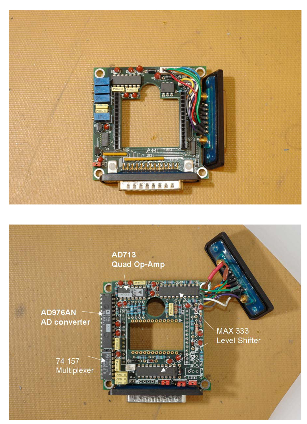 Figure 2:An assembled camera without the housing case. Clearly seen is the upper board with the CCD sensor (KAF 0402ME) inserted. Below it is the lower board and below that the cooling assembly including the peltier cooler (not seen) and the fan assembly.  The students are provided with all the components and instructions to fabricate this peltier cooled, computer controlled CCD camera. Most of the components are fairly easy to obtain through electronic resellers at a moderate cost or they can be obtained as a package of components from Genesis. An additional benefit of building the Audine designed camera is that there are many news groups dedicated to issues surrounding construction of this system. Students in this class have interacted with other builders of these cameras from around the world. The third class in the sequence is called “Testing of a CCD Camera” (SIMG 742). This class has two portions a one hour-a-week class and a 10 hour-a-week laboratory. Both portions are presented over the ten weeks of the Spring Quarter (March through May). Students are asked to conduct a series of calibration experiments similar to what they might be asked to do in a commercial, government or academic laboratory. The class time is used to present an overview of each calibration experiment and in the subsequent week to review the results obtained. Students generally use the camera fabricated in the prior quarter to conduct these fundamental testing experiments. The calibration experiments attempted include;
Figure 3:Two students from the class of 2006–07 (Michael Harris and Katelyn Kern) are shown experimenting with their completed camera. The camera is the gold colored box behind the Nikon lens that is directed at a resolution target mounted on the optical rail. The students are rarely seen as serious-looking as they appear in this photograph. 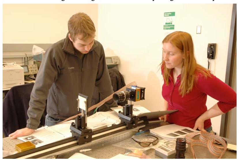 OutcomesOne surprise has been the diversity of students that have enrolled and successfully completed the classes. The 2007 incarnation of this class sequence has students enrolled from four different RIT Colleges, namely the College of Science, the College of Engineering, the College of Information Technology and the College of Imaging Arts & Sciences. These are students that rarely take a class together at any time during their undergraduate programs as even introductory courses in mathematics and science are now tailored to specific majors. The students in the laboratories are organized into diverse teams of three to build the camera. They generally come to appreciate, as they progress further into the building of the camera, that each student’s background is of value to the completion of the task. For example, a Electrical Engineering student knows more about circuit layout, an Information Technology students knows more about compute interface, an Imaging Science students knows more about data handling and analysis, and a Photography student knows more about optics. The elitist mentality (i.e. that one’s own major is superior to others) that often results from being confined into increasingly siloed academic programs is seen not to be true when building a complex instrument like a CCD camera (i.e. students discover that other majors know things that they haven’t learnt). Assessment for the first course in the sequence (i.e. Principles of Solid State Imaging Arrays) is achieved by a series of homework problem sets, a final examination, and a class presentation of fifteen minutes duration on a type of focal plane detector array that was not covered in class. A list of possible detector array topics to choose from is provided to the students. In addition for each topic a reference to a seminal paper is provided. Students are expected to utilize the electronic databases (e.g. INSPEC, SPIE Digital Library) available in the RIT library to find additional material. The key element of their presentation must be an explanation of the underlying physics governing the operation of the device and a clear illustration (i.e. a figure) of how the detector works. The homework assignments presume that the student has a working knowledge of one of the many higher level computational software packages available (e.g. MathCad, MathLab, Mathematica, etc.). The reason for this is that the problems are elaborate and much time can be saved by not solving the problems by hand or using a lower level programming language. The assessment for the second course (i.e. Fabrication of a CCD camera) involves a midterm exam, a final exam, maintaining an up-to-date group laboratory notebook, and a final oral exam. The final oral exam is key in a hands-on group project like this to ensure that all students have acquired a minimum knowledge of all areas of construction. The oral exam for this course is often the first time the students have had to respond directly to questions about their work. They are put on the spot and for some the experience is stressful. However it also gives them a taste of what to expect after graduation. The third class (i.e. Testing of a CCD camera) is assessed by means of a final exam and through the submission of detailed reports and conclusions on each of the laboratory tests the students complete. Since a commercial CCD sensor is used in the camera system the performance metrics determined by students as part of their laboratory can be compared to the specifications listed by the manufacturer. In some cases differences have been found and we have contacted the manufacturer for clarification. In more than one case the difference was found to be the result of an error by the manufacturer in their claimed performance. There is a sense of personal accomplishment when a student is able to build their own camera, knows how to operate it, and understands the underlying physics. The advantage to building a camera is that the students have personal knowledge of the assembly, and techniques of testing the device. If the unit doesn’t operate as expected, the student will not treat the camera as a black box but rather open the unit and probe for the problem. The building of the camera requires study of all aspects of the acquisition of an electronic digital image. This include: electronics, optoelectronics, data processing, mechanics, refrigeration engineering technology, optics and image processing.. Students who construct their own imaging systems have an excellent understanding of any similar instrument’s operation. This type of course is often cited by employers as the type of hands-on, practical course that is highly desirable for their future employees. University curriculum committees also like these sort of “capstone” courses where the years of conventional coursework are integrated with a hands-on experience into something meaningful and practical for students. However this sequence of classes requires a substantial investment of time by the faculty member responsible. Additionally the sequence of classes flows best when one faculty member is responsible for all three classes. The classes also involve a substantial financial commitment each year by the university to permit purchase of the components and to dedicate the laboratory space needed for the class. It is impractical to share the laboratory space with other classes as the cameras and test equipment are left in various states of assembly over the quarters and the laboratory times are individually scheduled by the groups so as to not interfere with one another. The commitment of an institution to providing their students with excellent technical higher education is revealed by their support of programs such as this. AcknowledgementsMany colleagues have assisted in the development of this course sequence. In particular I would like to thank Professor Roger Easton who has always been happy to listen to problems and help with solutions. All the administrative directors of the Center for Imaging Science have been encouraging of this program including, most recently, Ian Gatley and Stefi Baum. I also thank the many students who have taken the class who have been so enthusiastic and who have tolerated the inevitable snafus with understanding. Rick Smith at Genesis CCD has been helpful with his advise and assistance. ReferencesBerry R., Karito V., and Munger J.,
“The CCD Camera Cookbook,”
Willmann-Bell,
(1994). Google Scholar
Smith R.,
(2007) http://www.genesis16.org/mirror/ Google Scholar
[AUDE - l’Association des Utilisateurs de Détecteurs Electroniques,
(2007) http://www.astrosurf.com/audine/English/index_en.htm Google Scholar
|


