

|
|
1.Introduction1.1About Cal Poly.California has two university systems: the University of California (UC) system and the California State University (CSU) system. The UC system provides for undergraduate programs as well as advanced degrees and major research programs at all graduate levels. The CSU system offers Bachelors and Masters degrees in most of its departments but in general does not offer Ph.D. programs except in education. California Polytechnic State University (Cal Poly) is a member of the California State University (CSU) system. The CSU system has 417,000 students at 23 campuses around the state. Cal Poly has a full time enrollment of about 18,000 students. The engineering college is the largest on campus with 4,500 students. Cal Poly is located in San Luis Obispo, CA. This location is equidistant (4 hour drive) between the major metropolitan areas of San Francisco to the north and Los Angeles to the south. Cal Poly attracts approximately equal numbers of students from the northern and southern halves of California. The authors of this paper are from the department of electrical engineering (EE) and the department of Physics at Cal Poly. This paper will focus on major photonic education and research activities in these departments. The EE department has approximately 650 students enrolled and its sister Computer Engineering (CPE) department has 450 full-time students. There are 28 full-time professors in the EE department with 5 full-time equivalent lecturers. Within the electrical engineering department, there are four professors who are active in photonics education and research. The Cal Poly Physics department has an enrollment of approximately 120 undergraduate students. About a quarter of the twenty two full-time tenured/tenure-track faculty have research and professional development activities in the area of photonics. 1.2Key Issues for Photonics Education at Cal Poly.Cal Poly as a university has advocated the philosophy of “learn by doing” and has used this phrase in its marketing program for incoming students for several decades. A visit to the campus web site, www.calpoly.edu, will find the words “learn by doing” in the very center of the main page. It is part of this university’s culture to advocate a hands-on approach to learning. There is continuing debate among engineering faculty and administrators on how we continue to innovate and improve our student’s educational experience and educational outcome. The college of engineering has chosen to further invest in project-based learning programs for our undergraduate and graduate students as one of its key initiatives. A key action has been to establish a Project-Based Learning Institute (PBLI1) on campus. The goal of this program is to facilitate interaction between the university and industrial collaborators in order to create more multidisciplinary team-based opportunities for our students and faculty. The photonics area is a broad field that requires technical knowledge in quite a range of sub-disciplines. It certainly is a prime example of a field where contributors can come from a wide range of backgrounds. Photonics applications in communication, scientific, commercial, biological, and defense areas are all important to the California economy. A major challenge for Cal Poly is then to make sure our graduates interested in the photonics area have the multidisciplinary and team skills necessary to work in the diverse areas of photonics applications. Our photonic education program at Cal Poly emphasizes four main educational tools; A. Lecture Classes, B. Photonics Laboratory Classes, C. Student Photonics Club, and D. PBLI design projects. In this paper, we will describe these four items with emphasis on our new initiatives for part B and D. 2.Photonics Lecture and Laboratory Course Innovations at Cal PolyThis section describes the lecture courses and laboratory courses that are offered in Cal Poly’s photonics program. Special emphasis is given to contents of several of the laboratory courses to highlight some of the changes that have been made to improve our laboratory educational experience. Table 1 gives a summary of the lecture and laboratory courses offered in photonics at Cal Poly. Table 1:Photonics Courses Offered at Cal Poly.
2.1Photonics Lecture/Laboratory Offerings in Electrical Engineering:The EE department offers 3 undergraduate lecture/lab courses and 2 graduate lecture courses in the photonics area. Cal Poly has a 600 square foot photonics laboratory that is used both as a teaching and research facility. Figure 1 shows a photograph of one of three identical teaching optical benches that are used for undergraduate education. This laboratory was first established in 1986. A major upgrade occurred in 1995 to track some of the innovations in the fiber optic communications field. Laboratory equipment was financed primarily through generous equipment donations. We are also supported from the University for space, utilities, and equipment maintenance. Approximately 100 students take these EE undergraduate elective courses in photonics over the duration of a year. A second major upgrade of these laboratories is in progress. A brief description of each of these courses follows. Figure 1:Undergraduate photonics teaching laboratory station. This is one of three identical benches used in two of our undergraduate laboratory courses. The room is 600 square feet. It also accommodates a photonics research bench. In this particular exercise the students are measuring the modal dispersion-limited bandwidth of a multimode optical fiber at 850nm.  2.1.1EE403 Fiber Optic Communication (3 credit lecture)This course offers an introduction to fiber optic communication. The topics covered include propagation of light in optical fibers, attenuation and bandwidth, LED and laser diode sources for use with optical fibers, optical sources, detectors, and receivers. Design of optical communication systems with applications in telecommunications and local area networks (LANs) is covered. One of the prerequisites to this course is the Physics optics course, PHYS 323. EE 443 Fiber Optics Laboratory (1 credit)This laboratory course is a concurrent and companion course to EE 403. The topics covered in the experiments include experimental investigation of the properties of optical fibers, sources, and detectors. Measurement of numerical aperture, attenuation, bandwidth of optical fibers, and coupling of light into optical fibers are part of the experiment set. The specific experiments are: Experiment 1: Handling Fiber, Numerical Aperture. This involves cutting, stripping, and cleaving of fiber. Several fiber types are mounted on a bare fiber connector adapter and the numerical aperture is measured. A customized motorized scanner/detector was developed as a part of an earlier senior design project exercise. Experiment 2: Fiber Attenuation, Splicing, and the OTDR. In this experiment, fiber attenuation is measured using the cut-back technique. The Optical Time Domain Reflectometer (OTDR) is then used to measure loss of the fiber and of optical connections. The students also learn how to join optical fiber ends with a fusion splicer. Experiment 3: Single Mode Fibers, Source Output Characteristics. This experiment concentrates on the spectral characteristics of optical sources. Optical spectrum analyzer measurements are made for various sources such as LEDs, Distributed Feedback (DFB), and Fabry-Perot (FP) laser sources. Experiment 4: Sources, Coupling to Optical Fibers. In this experiment, the students couple the output of a laser component to a single mode fiber using an XYZ coupling adjustment stage. This enables students to fully appreciate the alignment difficulties associated with single-mode fiber components. Experiment 5: Bandwidth of an Optical Fiber. In this experiment, students measure the dispersion-limited bandwidth of multimode optical fiber. Both frequency domain and time domain measurements are made. In the last two years, additional experiments and upgrades were made to the EE443 fiber optic communication laboratory.
2.1.2EE418 Photonic Engineering (3 credit lecture)This course covers classical optics topics including electrooptic, accoustooptic and magnetooptic modulation and other interactions of light with materials. Modern optical design methods with emphasis on the use of computers to design simple optical systems and evaluate existing optical designs are part of the coursework. Paraxial and exact ray tracing through thin and thick lenses, mirrors and prisms, radiometry and photometry are covered during lecture. As part of the homework exercises, students use the Z-MAX ray tracing program installed in the photonics laboratory to design simple photonic imaging applications. EE458 Photonic Engineering Laboratory (1 credit)This laboratory course is a concurrent and companion course to EE 418. The topics covered in the experiments include experimental investigation of the techniques used in processing of optical signals. Examples are experiments on electro-optic modulation and acousto-optic modulation, construction of an RF spectrum analyzer, analog processing of optical signals, and charge-coupled array devices. Acoustooptic modulators are also used to make a simple scanning spectrometer. Many of the experiments span two weeks. Specific experiments include: Experiments 1: Acousto-Optic Modulator. In this two-week experiment, students explore the intensity modulation and beam deflection properties of an acousto-optic device (Bragg cell). They measure some parameters of an acousto-optic modulator, including Bragg angle, modulation bandwidth, and diffraction efficiency. Experiment 2: PIN Photodiode. In this two-week experiment, students investigate the properties of a PIN photodiode. Students determine the PIN responsivity, bandwidth, RC time constant, the noise equivalent power dark current, rms shot noise due to dark current, and signal current. Useful receiver circuits are constructed using this device. Experiment 3: CCD Photodetector Array. In this two-week experiment, students investigate the properties of a 2048x1 linear CCD array, and measure some of its important parameters. Some of the parameters of the CCD measured include the linearity and dynamic range, the dark current and noise, the charge transfer efficiency, bandwidth, etc. The students also use the CCD to measure the size of a very small object such as the diameter of an optical fiber. Experiment 4: Acousto-Optic RF Spectrum Analyzer. In this experiment, students simulate the design of an acousto-optic RF spectrum analyzer using the optics lab design software. The design is then constructed. Finally the students evaluate its performance using a linear CCD array, and a collimated Helium Neon laser beam. 2.1.3EE 422 Polymer Optoelectronics (1 Credit, Laboratory)This undergraduate laboratory offers students the chance to fabricate an organic polymer light emitting diode (LED). Simple photolithography and spin-on polymers are used to construct a working polymer LED. The same laboratory includes complete characterization equipment for the LEDs that each student constructs. 2.1.4EE520 Solar-Photovoltaic System Design (3 Credits, Lecture)This graduate course introduces the student to system design and applications of photovoltaic systems. It is open to senior undergraduates with the permission of the instructor. Topics covered include solar cell and storage battery theory, examination of insulation, variability and optimization techniques, principles of grounding protection and control, a survey of power conditioning equipment, and system integration techniques. 2.1.5EE530 Photonic Systems (4 Credits, Lecture)This graduate course employs a systems approach to photonics. Topics covered include design of radiometric information optics and imaging systems, remote sensing, guidance and tracking; fiber optics and laser communications; component modeling, optimization of systems for detection of radiant flux with maximum signal-to-noise ratio, modeling of sources, and optical systems; signal conditioning, and output display. 2.2Photonics in the Physics Department.Unusual for a Physics Department, Cal Poly has a required junior-level optics course (Physics 323). This course, which includes a lab, covers the basics of physical and geometrical optics. An elective junior-level course in laser physics (Physics 315) is also offered. A senior level course in optics (Physics 423) is offered once every two years and is taken by anywhere from eight to twenty students from various departments. It also has a laboratory component and within the constraints of the curriculum can cover a wide variety of topics at the instructor’s discretion. Recent topics have included Fourier optics, dielectric waveguides, computer generated holography and optical trapping. Although the Physics Department has no graduate students, this latter course often includes graduate students from Engineering. Exposure to other optical topics in the curriculum takes place in other courses. For example, in the year-long sequence of “quantum labs” (Physics 340-1-2) taken in the junior year students carry out experiments in photon counting, optical pumping, and high-resolution spectroscopy. 3.Student Photonics ClubIt has been our experience that it is important to give students a group identity. A student photonics club was formed in 1986 so that students who had an interest in photonics could have a common forum to talk about the subject and bond together as an entity. Figure 3 shows a picture of the initial group of students that formed the club in 1986. Several national and international professional organizations are available for student club affiliation. Our student club chose to be affiliated with SPIE. A major reason is the generous funding that SPIE offers for its student organizations. This funding is key for providing food at meetings and paying for event expenses throughout the year. SPIE also offers 2 major conference events that are within driving distance of Cal Poly each year. Photonics West is in San Jose (3 hours north) each January and the SPIE annual meeting is held in San Diego each August. Both of these events offer great opportunities for students to observe first-hand the diversity of the photonics field. We have recently chosen the on-campus name for this club as the RF, Microwaves, and Photonics club (RMAP). This broader title allows us to attract a wider range of students and encourage a better understanding of the diverse range of photonics and its applications. Student trips to industrial sites are provided about once per quarter. The group meets bi-weekly and often features guest speakers on a range of photonics related topics. Figure 3:This photograph was from the first student photonics club at Cal Poly in 1986. The picture shows a funding check from the SPIE being handed over to the student leadership from Professor Wollman.  A major focus of the club each year is to provide a display at Cal Poly’s open house celebration. Annual crowds of over 25,000 people gather together on campus to see activities from the departments and student clubs. The entire event is student managed. This activity again helps form an identity for those students interested in the photonics field and offers new students, parents, and their siblings a chance to see photonics in a fun-filled hands-on display. 4.Project-Based Learning and the Project-Based Learning InstituteThis section of the paper will describe what Cal Poly and the photonics group is doing to support the “learn by doing” label of the University. First a description of our long-established senior-project program and master thesis program is given. The college of engineering is embarking on a formalization of the use of projects as a learning tool. The Project-Based Learning Institute has been established to facilitate the linkage of industry with the college of engineering. These collaborations offer a wider range of student projects including interaction with industrial sponsors. 4.1Senior Design Projects at the Undergraduate LevelEach senior is required to have a two quarter long senior design experience as a requirement for graduation. Students can bring in their own vision for a project. They can also work in conjunction with projects sponsored by professors. A senior project handbook has been developed to guide the student on the expectations for completing a senior project. The results of the senior project program in terms of an educational outcome have been positive but highly variable. For the student who has a high degree of motivation and self-discipline, professors are often surprised at what can be accomplished over such a short period of time. On the other hand, there are students who are distracted in their focus and feel that the senior project program is an obstacle that must be overcome rather than an opportunity. The desire for a more uniform senior project experience has been an issue that has been discussed at the college of engineering level. It is also desired to bring in more projects that can directly impact relevant problems from industry. Several program changes have been made to address the need for a uniform experience in a multidisciplinary and team-based environment. The electrical and mechanical engineering programs are advocating cross-program teams to work together and receive senior project credit in their respective departments. The photonics team has recently completed their first joint senior project with mechanical engineering utilizing a 4 person optical, mechanical, and electrical design team to construct an optical coherence tomography subsystem. A wide variety of photonics related senior projects are active each quarter. The Physics department has a senior project requirement for graduation and students work closely with a faculty member for two quarters. This feeds into the faculty professional development requirements and the optics projects are usually well subscribed. There are a variety of research projects ranging from computational studies of pattern formation to experimental investigation of optical methods for fluid flow measurement. Several interdisciplinary projects are also underway including the use of optical tweezers for measuring bacterial adhesion (in collaboration with Dairy Science) and fluorescence measurement of phytoplankton in the ocean (in collaboration with Biological Sciences). 4.2Photonics Projects at the Graduate LevelAs a large undergraduate university, we continue to develop a variety graduate research projects through five major channels:
Figure 4.James De Leon standing by his master thesis setup of multimode fiber characterization for an industrial partner. 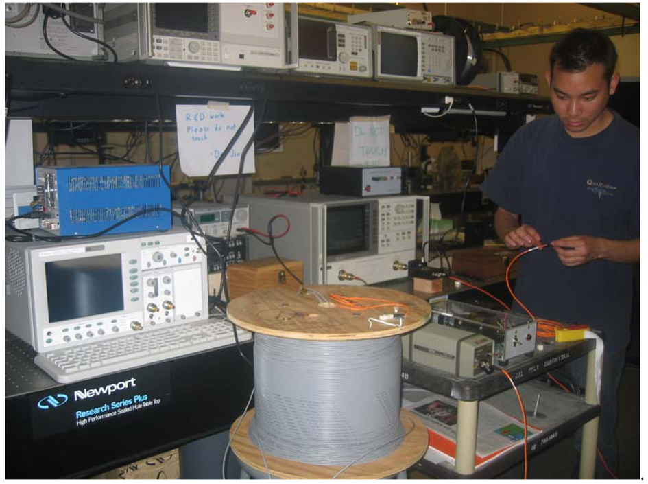 A large group of our Master’s degree students take advantage of Cal Poly’s 4+1 program. In this program the student forgoes the senior project and replaces it by a three quarter research program and graduate coursework. 4.3Formalization of Project-Based Learning Through the Project-Based Learning Institute (PBLI).Many professors have established direct relationships with industrial partners in order to provide interesting problems and research topics for undergraduate students. It takes a significant effort to cultivate these relationships. Once a track record of success has been achieved with the industrial partner, both groups see the benefits of working together and future projects become easier to maintain. The photonics group has worked to establish on-going industrial relationships. Lawrence Livermore National Laboratories has established a yearly project internship program with Cal Poly that has resulted in several Master’s degree dissertations as an example. The project based learning institute (PBLI) at Cal Poly was formed in the fall of 2006. The PBLI has a goal of formalizing the interface between the university and industry for project-based collaborations. A company that would like to work with the university now has a clear path to establish a project-based relationship with Cal Poly. The PBLI consists of permanent staff, established departmental project and research facilities, and the new Bonderson Student Project Center (see Figure 5). A major milestone in the establishment of the PBLI was the construction of an 18,000 square foot building for student projects. Paul. Bonderson (the building donor) was inspired by some of his senior project work and the path of success it gave for him in his career. The Bonderson Project center is 100% dedicated to project-based learning. Emphasis is given to multidisciplinary projects in conjunction with industrial sponsors. The building opened to students in March of 2007. The facility is being opened to students 7 days a week and 24 hours a day. The first Photonic-content project associated with this new project based learning institute is a prototype integrated small-scale air defense system using laser-based tracking of targets. The PBLI maintains a list of departmental competencies and individual professors’ interests that can be used to locate areas of potential interest overlap with industrial sponsors. The photonics area is highlighted as a featured area of competency to perspective industrial partners. PBLI also helps establish agreements on intellectual property ownership. The PBLI is funded by membership in the institute. A membership fee is charged for each participant. For this membership fee, a designated set of projects can be done in cooperation with the Cal Poly. Figure 5:The Bonderson Project Center of the Project-Based Learning Institute. This photo was taken in the March of 2007. The facility has become available for student projects as of March 2007. The facility is 18,000 square feet and is available 24 hours a day 7 days a week for undergraduate and graduate project work. Emphasis is given on multidisciplinary projects sponsored by industrial partners.  5.ConclusionThis paper gives an overview of the photonics program offered at Cal Poly. Specific coverage is given on how our photonics group has structured its undergraduate and masters level photonics programs. The laboratory contents and some of the recent upgrades are described in detail. Our view of photonics education emphasizes the importance of multidisciplinary project-based learning efforts as an educational tool. Student photonics organizations have been established to help forming a bond between students with a common interest. Finally, the photonics program is utilizing the college-wide project based learning institute to facilitate project-based learning interactions with industrial partners. Acknowledgements:Authors wish to acknowledge contributions from Dr. Zahed Sheik, director of the project-based learning institute. References:More information on Cal Poly’s project based learning institute can be found at www.pbli.calpoly.edu Google Scholar
Information on optical transceivers can be found at optical component supplier web sites such as www.finisar.com Google Scholar
application notes of LaserMOD are found at the RSOFT web site,Rsoft design Inc., http://www.rsoftdesign.com/ Google Scholar
|


