|
|
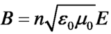
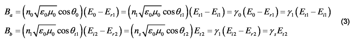
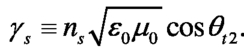
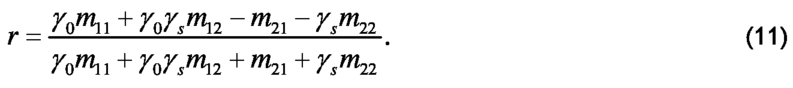
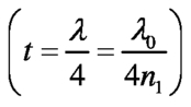
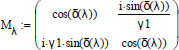
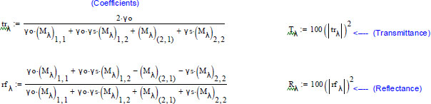
1.INTRODUCTIONIn the Introduction to Optics class students learn about the thin film1–5 concept through interference, (constructive and destructive interference), antireflecting coating, Michelson and Fabry-Perot interferometers. The course is taken by students in the spring semester of their second year after they have finished their introductory physics classes. The course is a three credit hour course with an accompanying lab that is one credit hour. In the same year the students are required to take the Programming and data analysis course in which, among other techniques, they learn how to use Mathcad. Since thin films are such an integral part of our daily lives, the purpose of these exercises is to give students a better understanding about the design and applications of thin films as related to optical filters. Other exercises related to thin films can be developed on the same structure. This paper highlights the concepts that students are introduced to as related to thin films and Mathcad exercises. While more sophisticated thin film analysis software packages6–8 exist, the purpose of these exercises is to encourage students to practice and combine their newly acquired knowledge of thin film concepts with the Mathcad skills to understand the importance of “theory and practice”. This will also make them be more comfortable and fast in their Mathcad programming and hopefully appreciate the ease with which Mathcad can simplify the tedious multiplication of matrices. 2.TRANSFER MATRIXThe transfer matrix is used to represent the film and characterize its performance. Its explanation and the subsequent theory presented below follows that which students are typically introduced to in undergraduate textbooks and follows that presented by Pedrotti.1 Mathcad will allow for calculations of net fields at one boundary of the film knowing the net fields at the other boundary. A one layer film is presented in the diagram below along with the components of the electric and magnetic fields of the incident, reflected, and transmitted wave. We assume a homogenous, isotropic film with index of refraction n1 deposited on a substrate with index of refraction ns and placed in a medium with n0. The incident beam undergoes an external reflection at the first interface (a) and the transmitted beam undergoes an internal reflection and transmission at the second interface (b). According to the boundary conditions, the tangential components of the resultant electric and magnetic fields are continuous across the interface, and where the magnetic field has tangential and perpendicular components. Using the relation where Et1 and Ei1 can be solved in terms of Eb and Bb: and finally, substituting the above expressions in the initial field components, obtain These expressions relate the field components at the first boundary to those at the next one and can be written in matrix form, where the numerical indices now indicate the boundary encountered by the wave as it passes through the system: Each layer of a multilayer coating has its own transfer matrix and the overall transfer matrix of the system is the product of individual transfer matrices, taken in the order in which the light propagates through the multilayer stack, Using the boundary conditions the transfer matrix could be rewritten in the form: The coefficients of reflection and transmission are defined as: These expressions can be used for any number of layers in a coating to determine the coefficients of reflection and transmission that can then be used to determine transmittance T = |t|2 and reflectance R = |r|2. 3.MATHCAD MODELING FOR REFLECTION AND TRASNMISSION CASESStudents will consider the most common case for thin films, that being normal incidence (θ0 = 0 rad). The phase difference becomes δ = (2π/λ0)n1t and the film has an index of refraction larger than that of the substrate. At normal incidence they can recalculate the expression for reflectance R 3.1One layer reflecting coatingA simple problem for students is to calculate the reflectance for a single layer. Example #1: A 50 nm thick film of TiO2 (n=2.40) is deposited on glass (n=1.50). What is the normal reflectance at a wavelength of 550 nm? The students easily compute the reflectance using the above equation to be 33.6%. However, a more meaningful calculation for them would be to determine reflectance over a range of wavelengths, using a Mathcad program. The program gives them flexibility to vary the index of refraction through choice of materials and analyze the effect of layer thickness on reflectance or transmittance. Figure 2 shows the Mathcad program for a single layer. The student begins by defining the necessary constants and conditions, such as the wavelength range, indices of refraction for the medium, film and substrate, and the layer thickness. Next follow the equations including the transfer matrix necessary for the calculations of the reflectance and transmittance, which can be computed and graphed simultaneously. Students can now see the behavior of the reflectance and transmittance over a wavelength range in the optical spectrum including the case analyzed in Example #1. For quarter-wave thick films The index of refraction, n1, for an antireflecting coating would then be 3.2Two-layer antireflecting coatingGiven the limited selection of materials for various indices of refraction, a double layer coating of quarter-wave films yields near zero reflectance at one wavelength. For normal incidence the transfer matrix is given by the product of the two transfer matrices that characterize each individual layer: The coefficient of reflection is then Example #2: A double layer of quarter-wave layers of CeF3 (n1=1.65) and Nd2O3 (n2=2.0) are deposited on a glass substrate (ns=1.52). The Nd2O3 layer is in direct contact with the glass substrate. Determine the normal reflectance for light at the wavelength 550 nm. Using the equation above the students can calculate reflectance to be 0.03%. But, by using the Mathcad program shown in Figure 3, they can easily analyze the reflectance and transmittance over the entire visible wavelength range to determine where the minimum reflectance and maximum transmittance occur. Building on the previous program they have to include the constants associated with the second layer (thickness, index of refraction, and transfer matrix) and perform the computation. Other cases that could be studied are double layer films built with combination λ/4 and λ/2 that broaden the wavelength range with low reflectance. The next step is to increase the number of layers to three. For each quarter-wave thickness, the zero reflectance occurs when 3.3High-reflectance layerOne can go to higher number of layers for high-reflectance coatings (such as the dielectric mirrors) and students are encouraged to practice on these films as well. In this case the order of the quarter-wave films is high index-low index with the stack repeated N times. The transfer matrix in this case is: and can be used in its general form in the Mathcad program as shown in Figures 4 and 5. Figure 4.Mathcad calculations of reflectance and transmittance for a high-reflectance multiple (N=2) stack.  Figure 5.Mathcad calculations of reflectance and transmittance for a high-reflectance multiple (N=6) stack.  Example #3: A high-reflectance stack incorporates six double layers of SiO2 (n=1.46) and CeO2 (n=2.35) films on a glass (n=1.50) substrate. What is the reflectance for light of 550 nm at normal incidence? In this example the students analyze the high-reflectance stack (dielectric layer) in which the order of the quarter-wavelength films is air – (high index – low index)N – substrate. Through simple computation students can determine that R=99.1%. However, by using Mathcad, students are now able to vary the number of stacks and analyze rapidly the change in the reflectance when N changes from 2 in Figure 4 to N=6 in Figure 5. Building on the previous Mathcad program for a double layer, the student has only to change the order of the layers (high index-low index) and how many times the double layer is repeated (N=2 or 6 in this example). 4.CONCLUSIONIn this paper we presented a Mathcad modeling exercise aimed to help students better understand the relation between thin films and transmission, reflection, interference, and their applications as related to optical filters. In addition, the exercises allow for a meaningful practice of their Mathcad skills acquired in their programming course. Constants Phase difference Transfer Matrix Transmission and reflection coefficients Constants Phase difference Transfer Matrix Transmission and reflection coefficients Constants Phase difference Transfer Matrix Transmission and reflection coefficients Constants Phase difference Transfer Matrix Transmission and reflection coefficients 5.5.REFERENCESPedrotti, Frank L., S.J. and Pedrotti, Leno S.,
“Introduction to optics,”
2ndPrentice Hall,1993). Google Scholar
Hechts, Eugene,
“Schaum’s outline of theory and problems in optics,”
(1975). Google Scholar
Heavens, O. S.,
“Optical properties of thin solid films,”
Dover Publications, Inc.https://doi.org/10.1063/1.3059910 Google Scholar
Heavens, O.S.,
“Thin film physics,”
T. & A. Constable Ltd,1970). Google Scholar
Fowles, Grant R.,
“Introduction to modern optics,”
2ndDover Publications, Inc.,1989). Google Scholar
|