

|
|
1.INTRODUCTIONThe Vertical-Cavity Surface-Emitting Laser (VCSEL) was first proposed in 1977 by Professor Kenichi Iga from Tokyo Institute of Technology, who two years later also achieved lasing for the first time under pulsed operation at 77 K.1,2 In earlier research by Ivars Melngailis in 1965, lasing parallel to the current injection was achieved for the first time and some of the advantages of this type of laser structure were highlighted such as easy array formation and low divergent output beam due to coherent emission from a large area.3 Room temperature operation in a VCSEL was achieved4,5 in 1989 and in the mid-1990’s VCSELs became commercially available. Today, more than 100 million VCSELs are produced annually and the price for such a laser for computer-mouse applications is approaching $0.10.6 Applications for today’s VCSELs include short-distance optical links, computer-mouse applications, laser printers, sensors, infrared illumination and tailored infrared power heating systems. They have become a popular light source because of their advantages over their edge-emitting laser counterpart such as high modulation speed at low drive currents, circular symmetric low-divergent output beam, low threshold currents, ease to fabricate into two-dimensional arrays, and low-cost manufacturing due to on wafer-testing.6 If VCSELs were also available with emission wavelengths in the ultraviolet to visible regime, many more applications could benefit from such a light source. For example, in visible light communication current state-of-the-art uses micro-light-emitting diode (LED) arrays. The performance of those emitters is limited by the spectral bandwidth and slow frequency response due to long carrier lifetimes associated with the spontaneous emission process.7,8 A laser would offer a light-source with a much narrower spectrum and much higher modulation speed. GaN-based edge-emitting lasers have been used to transmit 4 Gbit/s with a bit-error-rate of 2.7·10-4 in a 0.15m free-space link9 and more advanced modulation schemes (64-QAM OFDM) have been applied to reach 9 Gbit/s over 5 m in free-space10 with a bit-error-rate of 3.6·10-3. A VCSEL could offer additional advantages compared to an edge-emitting laser, as mentioned above. In solid-state-lighting, white light sources can be achieved by using blue LEDs with phosphorus coating to yield white emission. However, the blue LEDs are suffering from efficiency droop (reduction in power efficiency at higher drive current densities), and to efficiently generate enough lumens, an LED bulb must contain many LEDs where each is operated at a low-current density. This leads to a large part of the wafer being dedicated to just one LED bulb and results in a high cost. If blue-emitting lasers would be used instead of the LEDs, a high-power conversion efficiency could be achieved at much higher current densities, and the much higher optical output power generated by a single device would correspond to a smaller area to achieve the same lumens, resulting potentially in a lower cost for laser-based lighting systems.11-12 A VCSEL offers a more directional, circular-symmetric beam, which could lead to new and more compact luminaires at a low cost. In addition, the individually addressable elements in a two-dimensional VCSEL array would enable tailor-made, dynamic emission patterns for smart lighting systems. GaAs-based VCSEL arrays are established devices in laser-printers, and higher resolution, high-speed printers would benefit from VCSEL arrays with shorter emission wavelengths.13 Single-mode and polarization stable VCSELs might also be of interest in high-density optical data storage, most likely only for read-out where 4-5 mW is required, and not for writing where the power levels required are about 30-40 mW,14 much higher than what a single-mode VCSEL can deliver. GaN-VCSELs could also be of interest for laser display applications, such as head-up-displays, near-eye displays15 and picoprojectors, which do not require so much optical output power. Different sensor applications, such as Doppler-based interferometers16, could also benefit from a short-wavelength VCSEL. The interest for short wavelength (400-500 nm) lasers in bio-sensors and medical diagnosis and treatment is rapidly growing and new applications are continuously arising. Chemical tracking and biological agent detection is enabled by exciting fluorescent dyes and proteins.17 In dentistry, low power lasers are used to detect caries, using fluorescence from hydroxyapatite or bacterial by-products. Moreover, photochemical reactions based on photoactivated dye techniques can be used to disinfect root canals, periodontal pockets, cavity preparations and sites of peri-implantitis.18 In optogenetics, stem cells can be genetically modified to render them sensitive to blue light. Thereby, events in specific cells of living tissue can be controlled, with applications in artificial ears19 or eyes. Blue VCSELs could enable novel designs and facilitate system integration into the body. A 2D-VCSEL array would allow for selective stimulation of a nerve without mechanical repositioning of the laser and the individually addressable lasers gives the possibility to stimulate multiple sites simultaneously. This two-dimensional probing of neural networks has been demonstrated with GaN micro-LED arrays20, and is desired for example in chochlear implants21. Blue LEDs have recently been used in in vivo optogenetic experiments22, where VCSELs could offer additional advantages such as a low-divergent circular-symmetric output beam and improved high-speed performance. In the field of medical diagnosis, the detection of skin and esophagus cancer is now possible without the use of biopsy by using laser-induced fluorescence at a wavelength of 410 nm.23,24 GaN-based lasers have also recently been used in early diagnosis of oral cancer.25 This non-invasive technique is fast, reliable and reduces both pain and recovery time for the patient. In medical treatment, a technique has recently been developed which uses blue light to activate chemotherapy drugs in specific cells, which could lead to more effective chemotherapy for cancer treatment with limited side effects.26 To summarize, even though there are no commercial GaN-based VCSELs yet, there are many applications which would benefit from such a light source, and most likely more applications will appear once such light source is available. It is also encouraging to see many companies investing time and effort into this field, and as a result Nichia27, Panasonic28 and Sony29 now all have demonstrated electrically injected GaN-VCSELs. 2.STATE-OF-THE-ARTThe first electrically injected GaN-based VCSEL was demonstrated by the National Chiao Tung University (NCTU) in Taiwan in April 2008.30 It had one bottom epitaxial AlGaN/GaN DBR, one top dielectric DBR, and a 240 nm indium- tin-oxide (ITO) layer as a current spreading layer. It operated under continuous wave (CW) conditions at 77K at a wavelength of 462.8 nm. The threshold current density was 1.8kA/cm2 for a 10-μm device, and the output power was published in arbitrary units. The first room temperature CW operation was reported by Nichia Corporation, Japan, in December 2008.27 This device used two dielectric DBRs, a 50 nm ITO layer, and a device with an 8μm-aperture had a threshold current density of 13.9 kA/cm2 and an output power of 0.14 mW. Publications from a few groups followed, and since the first demonstrations there have been a lot of progress in the field of electrically injected III-nitride based VCSELs, both in terms of new technological solutions as well as performance characteristics.31 To date there are seven groups in the world who have demonstrated lasing under electrical injection27-30,32-47, and the different approaches and structures are summarized in Table 1. The performance characteristics of published devices, in terms of output power and threshold current density, are plotted in Fig. 1. To compare performance characteristics of lasers it is important to study both optical output power and threshold current since they are interlinked, for example a laser with a low top mirror reflectivity can have a high optical output power, but the threshold current would then also be high. To be able to compare published results from GaN-based VCSELs with different aperture sizes, current density instead of current is plotted in Fig. 1.This is however a measure that should be taken with caution, since the injection current and emission profile of GaN-based VCSELs are sometimes far from uniform across the whole aperture, due to filamentary lasing. Continuous-wave operation is indicated in the figure by filled markers and pulsed operation by open markers. The lasing wavelength is also different from case to case, which have been illustrated in the figure by three colored groups; violet (406 nm - 422 nm), blue (446 nm – 463 nm), and green (503 nm). Table 1.Different approaches and structures used in electrically injected VCSELs.27-30,32-47
*The penetration depth into the DBR is not accounted for. Figure 1.Optical output power and current density for electrically injected GaN-VCSELs published to date.27-30,32-47 Filled markers illustrate continuous wave operation and open markers pulsed operation. The colors indicate the lasing wavelength, violet (406 nm - 422 nm), blue (446 nm – 463 nm), and green (503 nm).  As seen in Fig. 1, there are now several reports on optical output powers close to 1 mW with decent current densities. These performance characteristics can be compared to that of the more mature GaAs-VCSELs emitting at 850 nm, where our standard devices with an 8-μm aperture size have a maximum optical output power around 4-10 mW depending on mirror design and a threshold current density around 0.8-2.0 kA/cm2. The performance of our GaAs-VCSELs with 9 and 11μm apertures are published in Refs.48,49. The comparison in performance characteristics between GaN- and GaAs- VCSELs, shows that there is still room for improvement for GaN-based VCSELs. A schematic view of an electrically injected GaN-based VCSEL is shown in Fig. 2, and as mentioned previously, the detailed structures are summarized in Table 1. Compared to a GaAs-based VCSEL there are some differences such as the use of one (or even two) dielectric DBRs in GaN-VCSELs due to the lack of a two near lattice-matched materials with high refractive index contrast. The DBRs are not electrically conductive, thus intracavity contacts are always used, and the cavity length is much longer in GaN-VCSELs. Due to the low electrical conductivity of p-GaN, transparent current spreading layers are necessary to allow for efficient current injection from the intracavity contacts to the multiple InGaN quantum wells. Indium-tin-oxide is in most cases employed, except for one recent publication which demonstrated a tunnel junction combined with highly conductive n-GaN on top as the current spreader37. Lateral current confinement has usually been achieved by a dielectric aperture of silicon dioxide or silicon nitride, and lately optically guided structures are also being explored and implemented. In GaAs-VCSELs simultaneous current and optical confinement is achieved by selective oxidation of a high Al-content AlGaAs-layer. Recently, new approaches for current confinement in GaN-VCSELs have been developed such as plasma damage of p-GaN32, ion implantation36,47, and airgaps by photoelectrochemical etching38. A number of key challenges in GaN-VCSEL will be described in more detail in the next chapter. 3.KEY CHALLENGES3.1MirrorsGaAs-VCSELs profit from the near lattice-matched AlGaAs-material system, which allows for growing crack-free highly reflective Distributed Bragg Reflectors (DBRs). The relatively high refractive index contrast (Δn/nhigh) of 14% at 850 nm for an Al0.12Ga0.88As/Al0.90 Ga0.10As DBR, results in a broad stopband of 75 nm (full-width half-maximum) for a standard bottom DBR with 34 mirror pairs. Since both mirrors in a VCSEL need a reflectivity above 99%, an even more relevant measure would be the width of the spectrum for a reflectivity above 99%, which is 59 nm for the mentioned DBR. Besides a high reflectivity over a broad spectral range, the AlGaAs DBRs can also be electrically conductive, allowing for current injection through the DBRs and contacts can thus be placed on top of the top DBR and on bottom of the bottom DBR. Achieving broadband, high reflectivity, electrically conductive DBRs in the III-nitride-based material system is a big challenge. It is difficult to find two materials with high refractive index contrast that are lattice-matched to each other, and in addition have high electrical conductivities. High peak reflectivities (>99%) have been reached with DBRs in (Al)GaN/Al(Ga)N50-53 as well as in AlInN/GaN54,55. An AlN/GaN DBR has a higher refractive index contrast (about 12% at 420 nm), which is close to that of AlGaAs DBRs, and as a result the 99% stopband width is about 22 nm if 22 mirror pairs are used. However, the DBR suffers from an in-plane lattice mismatch of about 2.5%. Ternary AlGaN could be used instead of binary AlN/GaN to mitigate cracking, but a larger number of pairs is then necessary to reach high enough reflectivity due to the lower index contrast, and the stopband width will thus be narrower. To reduce stress in the DBR, short-period superlattices (SLs) have been used, below the DBR56, and incorporated into the DBR52. The inserted AlN/GaN SLs can suppress the generation of cracks, but cannot reduce the number of the V-defects.57 Another way for strain management is to use thin low-temperature AlN interlayers.53 The interlayers can reduce crack-formation, but can also reduce the overall reflectivity of the DBR, which has to be taken into account when designing the DBR. Spontaneously formed interlayers have also been seen to reduce the peak mirror reflectivity and stopband.58 Selective area growth has also been applied to grow crack-free DBRs in areas up to 150x150 μm,59 sufficiently large for VCSELs. Instead of AlGaN, an epitaxial DBR can be realized using lattice-matched AlInN/GaN to grow strain free highly reflective mirrors60. The composition of AlInN is very sensitive to growth conditions, but if grown correctly, it can result in a basically strain-free DBR allowing for high quality quantum wells to be grown on top. The index contrast of the layers is however lower than AlN/GaN (about 6% at 420 nm), which results in a mirror with a more narrow 99% stopband of about 12 nm if 42 mirror pairs are used. Any deviation in thickness of the DBR layers will translate into a deviation in the center position of the stopband, for example a 3% thickness deviation, results in a 3% shift of the center position of the DBR stopband, which corresponds to 12.5 nm if the mirror is designed for 420 nm. As a result, the 99% stopband could end up outside the 99% stopband of the other DBR if one mirror has 3% thicker layers. Thus, a narrow stopband DBR makes the spectral alignment between DBR reflectivities more challenging as well as their matching with gain spectrum and cavity resonance. There have been very few reports on electrically conductive DBRs61-63 due to the low electrical conductivity of III-nitrides and the many hetero-interfaces necessary in the DBRs (due to the low refractive index contrast of the materials). Thus, intracavity contacts have so far been the only option for GaN-VCSELs. To avoid the problem with epitaxial DBRs due to the low refractive index contrast and non-lattice-matched materials, an alternative approach is to use dielectric DBRs. Due to the higher refractive index contrast (44% if SiO2/Ti2O2 is used) only about 11 pairs are required to achieve a high reflectivity and the resulting 99% stopband width is as wide as 148nm. A double dielectric scheme does however require either substrate removal or epitaxial lateral overgrowth of the bottom dielectric DBR, making the exact control of the cavity length challenging, see Section 3.3. Substrate removal has been achieved by laser-induced lift-off, polishing and photoelectrochemical etching (PEC) of a sacrificial layer. Laser-induced lift-off is not easily applied to VCSEL structures grown on free-standing GaN, due to the lack of absorption contrast between epitaxial GaN and the GaN substrate. Insertion of light-absorbing structures is possible but might hamper the crystal quality of the VCSEL structure grown on top, since they are usually not perfectly lattice-matched to GaN. The fabrication process requires bonding to a support substrate to be able to handle the thin layer structures that are lifted-off and the layer structure has to have a certain thickness, typically above 4 μm to avoid stress fractures in the GaN film.64 Chemical mechanical polishing (CMP) on the other hand can be applied to remove GaN substrates from epitaxial GaN structures. However, thickness control is a challenge, as is achieving low-thickness variation across a large-area substrate due to the hardness of the GaN material. This method also requires bonding to a support substrate. PEC also requires bonding, but has the advantage of providing a more accurate cavity length control. ELOG does not require bonding, but achieving short cavity lengths and an exact control of the cavity length is challenging, due to the ratio between vertical to horizontal growth rates. Besides the above-mentioned challenges with a double dielectric DBR scheme, it will in addition lead to VCSELs with increased heating thereby faster misalignment of cavity resonance and gain peak, due to the lower thermal conductivity of dielectric DBRs. Dielectric DBRs have a high refractive index contrast, but an even higher contrast (Δn/nhigh=60%) can be achieved if the DBR consists of GaN and air. In this case only a few periods would be necessary to achieve a high reflectivity, and the stopband will be very broad. In the realization of a semiconductor/air gap DBR, selective wet-etching is crucial as every second layer (sacrificial layer) in the DBR has to be removed to create the air gaps. Unfortunately, III-nitrides are chemically stable in most solutions and thus very difficult to wet etch. There have been a few demonstrations of GaN/air- DBRs, utilizing wet-chemical etching of AlInN65,66, combined electrochemical oxidation and wet-chemical etching of AlInN67 or photoelectrochemical etching of InGaN68, and electrochemical etching of n-doped GaN69,70. Most critical in the fabrication of GaN/airgap DBRs is to avoid collapse of the structure and to achieve a mechanically stable structure with no bending. The thickness of the GaN is often increased to 5λ/4 instead of λ/4 to improve mechanical stability. Another challenge is the often low selectivity in the wet-etch, which results in a non-uniform thickness of the GaN layers in the radial direction, since they are slightly etched in the removal of the sacrificial layer. An alternative to a DBR is a high refractive index contrast grating (HCG), which is described in more detail in Section 5. HCGs are believed to offer a number of advantages71, such as transverse mode and polarization control and a broader reflectivity spectrum than epitaxially grown DBRs. An additional benefit is the possibility to set the resonance wavelength of the VCSEL by the dimensions of the grating72, which recently was demonstrated in a GaAs-based VCSEL73. By varying the duty cycle and/or the period of the grating, while maintaining the same grating layer thickness, the phase of the reflected wave can be altered without affecting the magnitude of the reflection. A change in phase is effectively the same as changing the cavity length, i.e., by varying the lateral parameters of the grating on nearby VCSELs, individual resonance wavelengths can be achieved for devices from the same epitaxial layer structure. Thus, enabling the fabrication of a multi-wavelength VCSEL array where the emission wavelengths of the individual devices are set in one single post-growth lithography step. A main challenge in the fabrication of a III-nitride-based HCG is to find a sacrificial layer that can be selectively removed without affecting the HCG layer. There have been a few attempts, such as bandgap-selective photoelectrochemical etching of a sacrificial InGaN superlattice to form an AlGaN HCG membrane74 however, with a limited airgap height, and focused-ion-beam etching to create an airgap underneath a GaN-based HCG75, an impractical process for device integration on a wafer-scale. In addition, GaN membrane gratings have been fabricated from a GaN-on-Si structure76-78 by selective etching of Si, and free-standing hafnium-oxide gratings using the same approach79, but applying this concept to fabricate a bottom mirror in a VCSEL is not straightforward, since growth of high-quality GaN on Si for laser applications is very challenging. Due to the difficulties in realizing a III-nitride based HCG structure with an airgap, a grating reflector without an airgap could be used, which previously has been proposed for long-wavelength VCSELs where the mirror fabrication also is complex.80 Such a reflector in GaN has been demonstrated.81 This concept offers a more mechanically rigid structure, but the lower index contrast results in a much smaller fabrication window to achieve a reflectivity above 99%. An alternative approach for an HCG for III- nitride-based light-emitters is a free-standing dielectric HCG in TiO2 realized by a sacrificial SiO2 layer82. It offers approximately the same high index contrast as that of free-standing GaN HCGs, since the refractive index of TiO2 is about 2.6 at a wavelength of 450 nm, with a negligible absorption for wavelengths above 400 nm. In addition, the TiO2 HCG scheme allows for direct integration into many different material systems, since lattice-matching is no longer a prerequisite. 3.2Carrier transport and optical gainCarrier transport must be optimized along both the vertical and lateral directions in order to achieve uniform carrier distribution among the multiple QWs of the active region and within each QW defined by the current aperture. A vertically uniform carrier distribution among the QWs is a challenge in all GaN-based light-emitters83,84 due to the large difference between the activation energy of donor and acceptor impurities85, the strong imbalance between electron and hole mobilities86, the large band offsets and, possibly even more critical, the spontaneous and piezoelectric polarization effects at heterointerfaces87,88. In order to maximize the radiative recombination in the QWs, one should minimize current crowding89,90 as well as carrier leakage beyond the active region, which can involve both electrons91-93 and holes94 and could be enhanced by Auger95,96 and excited subband recombination97. Electrons can be prevented from leaking into the p-GaN layers by inserting an energy barrier in the conduction band between QWs and p-layers, a so- called electron-blocking layer (EBL). However, an EBL will also affect hole injection into the QWs, and the EBL design is thus crucial for low-threshold operation. Many different EBLs have been proposed and their effect on VCSEL performance has been investigated such as different p-doping levels of the EBL98, compositionally graded EBL99, and multiple barrier EBL100. The design of the active region is very important, and Table 1 summarizes the different approaches used in electrically injected VCSELs. It is clear that there is so far no consensus on how the active region should be designed. For example, having many QWs (up to 10 have been used) may increase the optical gain per roundtrip in the cavity and the tolerances to spatial misalignment between the maximum of the standing optical wave and the QWs. One drawback is the nonuniform carrier distribution among QWs due to the above-mentioned mechanisms; as a result, it may occur that only the QWs nearest to the p-side contribute to the optical emission, as observed experimentally in InGaN/GaN LEDs101 and predicted by simulations of GaN-based Fabry-Pérot lasers102 and VCSELs103. This reduces the net gain since QWs that are pumped below transparency absorb light. The use of fewer QWs can lead to a more uniform carrier distribution between QWs, but could also result in an increased electron leakage104. Numerical simulations have shown that the insertion of a tunnel junction (TJ) in the middle of 10 QWs could improve the uniformity in carrier distribution and lead to higher output power105. Another approach to achieve more uniform carrier distribution106 and higher optical gain107 is to grow on nonpolar or semipolar planes rather than along the c-plane. III-nitride-based materials have, unlike GaAs, strong built-in electric fields due to spontaneous and piezoelectric polarization. In the QWs, the large electric field perpendicular to the epitaxial layers spatially separates the hole and electron wavefunctions, which leads to a reduced wavefunction overlap and thus a reduced radiative recombination efficiency and an increased threshold current. An increased overlap between hole and electron wavefunctions can also be achieved in QWs grown on polar planes by tailoring the shape of the QW along the growth direction. These are referred to as large-overlap QWs, and both step-function compositional grading108-109 as well as linearly grading110 have been proposed. However, an additional advantage with InGaN QWs on nonpolar and semipolar planes is the anisotropic optical gain leading to VCSELs with a preferred polarization state35 without the use of for example surface gratings111,112. To achieve low threshold currents, the optical mode must overlap well with the gain region defined by the current aperture. A laterally uniform carrier distribution within the gain region is also desirable to avoid selective excitation of higher order transverse modes. However, simulations show that due to the large difference in mobility between electrons and holes in III-nitrides, the recombination will predominantly take part in the periphery of the aperture and not in the center113. In addition, III-nitride VCSELs must use intracavity contacts due to the non-conductive DBRs. Thus, current spreading layers are necessary, and the transparent conductive oxide indium-tin-oxide (ITO) is most commonly used. However, ITO has a relatively high absorption (about 1000 cm-1), and must thus be placed in a minimum of the standing optical wave to keep the losses low. Any deviation in cavity length from design will dramatically increase the absorption losses. The surface roughness of the ITO should also be low, preferably having a root-mean-square < 1 nm to keep scattering losses low in the VCSEL114. Moreover, it is challenging to achieve a low contact resistivity between p-GaN and ITO, making it difficult for the contact to survive the high current densities required in VCSELs (typically tens of kA/cm2). ITO deposition, usually done by sputtering to achieve high quality115, can easily lead to plasma damage of the p-GaN116,117, preventing a low-resistive contact to be formed. Remote plasma deposition or physical vapor deposition such as electron beam evaporation can be used to avoid plasma damage of the p-GaN. In addition, multilayered ITO deposition at different temperatures has been developed to optimize contact resistivity, ITO properties118 and surface roughness114. Alternative solutions for a current spreading layer have been investigated, such as thin metal layers119 and graphene120. Metals have low sheet resistance and can provide low-resistive contacts to p-GaN, but have a strong absorbance. If made thin enough and placed very accurately at an optical field node the optical absorption loss can be relatively low, but any deviation from target position will dramatically increase the absorption loss. Moreover, the resistance in very thin metals is much higher than in bulk layers121 and their reliability and degradation at high current densities needs to be investigated. A single layer of graphene has an absorption loss of 2.3%122 in the visible wavelength range, and if placed accurately within the cavity it would lead to a relatively low loss. However, most graphene has so far been transferred to GaN-based LEDs, and as a result of the transfer the contact resistivity is poor. There have been attempts to grow graphene directly on p-GaN123,124. If such a technique can be developed that can provide graphene, or any other twodimensional material, with low resistance, high transparency and ohmic contact to p-GaN that can withstand high current densities, grown under conditions that do not jeopardize the underlying device structure, it may be a way forward. So far, though, the most promising approach to replace ITO is the tunnel junction (TJ). By incorporating a TJ, the topmost part of the p-GaN layer and the current spreading ITO layer can be replaced by a low-resistive n-GaN and the current spreading issue with associated high optical loss can be addressed. In long-wavelength InP-based VCSELs, which share many of the same challenges as GaN-VCSELs such as low p-type conductivity, high metal contact resistance to p-doped material, and poorly-conductive DBRs, tunnel junctions are a standard technology to achieve efficient lateral current spreading125. In order for the TJ to be successful in III-nitride-based VCSELs, in reverse bias it should have a low resistance with low additional voltage drop, low optical absorption and be able to withstand the high current densities. This has been a challenge in III-nitrides due to the large bandgaps and low hole concentrations. In recent work, TJs with thin InGaN layers have been explored to utilize the lower bandgap and polarization fields to reduce the tunneling barrier and facilitate the carrier tunneling126,127. However, the absorption losses, critical for VCSELs, must be investigated and will most likely be higher than if only GaN is used. GdN nanoislands have also been incorporated in the TJ interface to increase the tunneling through midgap states128,129. Very promising are the pure GaN TJs demonstrated recently which have been incorporated into LEDs130,131. They have shown low differential resistance for a complete device (low 10-4 Ωcm2), and ability to withstand current densities exceeding 20 kA/cm2. Buried tunnel junctions have also been demonstrated to laterally confine the current130, and if the introduced structural step from the overgrown TJ transfers into the top DBR, it might also provide simultaneous optical guiding132,133. In most III-nitride-based VCSELs, the main focus has been on lateral current confinement and not on optical confinement. However, to achieve an efficient device with low threshold it is important to ensure a good lateral overlap between the optical mode and the carriers in the QWs. In fact, it has been shown that most apertures used for current confinement result in optically anti-guided structures with associated high losses132,133, for more details see Section 4. Switching to index-guided structures instead, will contribute to lowering threshold currents and can be an effective way to reduce filamentation, something often seen in GaN-VCSELs27,28,30,32,39,40,46, and also seen in early proton-implanted gain-guided GaAs-VCSELs135,136. 3.3Cavity lengthTo achieve a VCSEL with a low threshold current it is important to ensure a good spatial overlap between the optical mode and carriers. In the lateral direction this is achieved by having an aperture(s) that confines carriers and optical field to the center of the device, and in the vertical direction this is done by placing the quantum wells (QWs) in a maximum of the standing optical wave. The optically absorbing regions, such as the ITO layer, should be placed at a field minimum, see Fig. 3. Besides this spatial matching, spectral matching between the cavity resonance, gain peak, and reflectivity of the mirrors is also required. A good control of the cavity length is of utmost importance since it will affect both spatial and spectral matching. Table 2 shows that most GaN-VCSELs use a cavity length (distance between the DBRs) of about 7λ or even longer. GaAs-VCSELs, on the other hand, use a shorter cavity length, even as short as 0.5λ, to improve transport and optical confinement in order to push the high-speed performance137-139. There are several reasons for using longer cavity lengths in GaN-VCSELs. The intracavity contacting scheme forces the use of a thick n-GaN to keep the lateral resistance from the n-contact layer low. If there is residual strain in the underlying structure, for example from epitaxial DBRs, the n-GaN must be grown to a certain thickness to allow for high quality QWs to be grown on top. If an epitaxial lateral overgrowth of the DBR is applied instead, the thickness of the n-GaN will be determined by the ratio between lateral and vertical growth rates in combination with the geometry of the overgrown DBR29. If chemical mechanical polishing is used to remove the substrate, the n-GaN will also be thick due to the inaccuracy in the substrate removal process28. In addition, a longer cavity length yields a decreased longitudinal mode separation, making it easier to match one longitudinal mode (or several) to the stopband of the mirrors and the gain spectrum. In a device with a 2-μm cavity length and two dielectric DBRs, the measured longitudinal mode separation was about 7 nm28, while the gain spectral width for InGaN QWs is below 15 nm140 for a carrier concentration of 3·1019cm-3 and the net modal gain will be even narrower. If epitaxial DBRs are used the refractive index contrast is less, and thus the penetration depth into the DBRs will be longer, yielding a much longer effective cavity length for the same physical distance between the DBRs. Thus, devices with one epitaxial DBR usually have a shorter longitudinal mode separation, but on the other hand the reflectivity spectrum that the mode has to fit within is narrower. Moreover, the resonance wavelength (λ) is less sensitive to deviations in cavity length (ΔL) for a longer cavity, i.e. Δλ=λΔL/L.28 This is an advantage since it is very difficult to control the cavity length within a few percent for a GaN-based VCSELs, no matter if epitaxial or dielectric DBRs are used. The drawbacks with a longer cavity are increased absorption loss in the cavity, reduced longitudinal confinement and decreased spontaneous emission factor. Figure 3.Standing optical wave inside the cavity for a GaN-VCSEL with an outcoupling DBR of 7-pairs of TiO2/SiO2 and a highly reflective DBR of 42-pairs of AlInN/GaN (top figure) and 11-pair TiO2/SiO2 (bottom figure).  The importance of an accurate cavity length is illustrated in Fig. 4 for the case of two dielectric DBRs and in Fig. 5 for and one dielectric and one epitaxial DBR. The structure and material data used are the same as in Ref.132, except for the bottom DBR, which in Fig. 4 consist of 11 mirror pairs of TiO2/SiO2 and in Fig. 5 42 mirror pairs of AlInN/GaN without any absorption losses. The calculations were performed using the one-dimensional effective index method141 and the deviation in cavity length corresponds to a change in the bottom n-GaN thickness that nominally is 904.4 nm thick. Negative deviation in cavity length corresponds to a shorter cavity length and positive deviation to a longer cavity length. The threshold material gain increases faster with a deviation in cavity length for the VCSEL with an epitaxial DBR, an increase of 100 cm-1 is reached already when the cavity length deviates by less than ±10 nm, while in the double dielectric DBR VCSEL the cavity length can deviate by more than ±35 nm before the same increase of 100 cm-1 occurs in threshold material gain. This is due to the fact that when the cavity length deviates from the optimum value, the resonance wavelength will shift, and will no longer overlap with the maximum reflectivity of the DBR. In the case of a low-refractive index DBR (as an AlInN/GaN DBR), this reduction in mirror reflectivity occurs much faster due to the narrower reflectivity spectrum. Due to the low-refractive index contrast of the epitaxial DBR, the penetration depth of the optical field into the DBR is longer, which results in a longer effective cavity length, and thus a shorter separation of the longitudinal modes. For the examples in the figures the longitudinal mode separation is about 18 nm in the case with one epitaxial DBR and 27 nm for the double dielectric scheme. The shorter longitudinal mode separation does not help much to reduce the threshold material gain required for the epitaxial DBR VCSEL, since it is dominated by the low peak reflectivity and narrow reflectivity spectrum. It can however help a bit in reducing the threshold current since the detuning between resonance wavelength of a longitudinal mode and the gain peak will be less if the longitudinal mode separation is less. On the other hand, if the longitudinal mode separation is too short, multiple longitudinal mode lasing can occur. It should be noted that the resonance wavelength shifts less with a deviation in cavity length for the epitaxial DBR VCSEL, due to the longer effective cavity length. The shift is about 7 nm for a thickness deviation of 30 nm in the epitaxial DBR VCSEL case, and 10 nm or the same thickness deviation in the double dielectric DBR VCSEL. A benefit with the epitaxial DBR is the higher thermal conductivity, which results in a smaller resonance wavelength shift with drive current due to a lower temperature rise, which also affects the overall laser performance. The increase in threshold material gain due to a deviation in cavity length will affect the laser performance, but is not big enough to totally prevent lasing in the case of a double dielectric DBR, since InGaN QWs have proven to be able to deliver a material gain above 2500 cm-1.140 However, in the case of a VCSEL with a bottom epitaxial DBR, the cavity detuning might in fact prevent the laser from reaching threshold. 4.GUIDING AND ANTIGUIDING EFFECTSIn the early works on electrically injected GaN-based VCSELs, the main focus on apertures was to obtain a good lateral current confinement without paying too much attention to the impact on optical properties 27,28,30,32,33,40,44,45. The method applied was to create an aperture by depositing an electrically non-conductive layer (often SiO2 or SixNy) on the p-GaN on top of the mesa and then fabricating a hole in the center onto which a transparent conductive layer (ITO) was deposited to pass the current through. In 2013, we reported our concern regarding these resulting non-planar structures134, i.e. having a downward step profile in the center (δ>0 in Fig. 7), referred to as a depression in the structure. It was shown that the degree of the depression (or elevation in the case of upward step profile, δ<0) is simply and directly related to the ability of the laser cavity to work as a good waveguide. An optimal design of the optical waveguide is of great importance to achieve a good lateral overlap between the optical mode and carriers and to minimize lateral diffraction and radiation loss. Figure 7.(Left) A schematic illustration of a GaN-based VCSEL structure having a dielectric current aperture. (Right) A scanning electron microscope (SEM) image of a structure with a depression δ in the center: Note that δ is the same as the dielectric layer thickness indicated at bottom right in the figure.  Fig. 8 shows the layer structure with a depression in the center and the standing optical wave pattern in the center of the device. For some lateral cross-sections, indicated by green dashed lines, the refractive index of the material is lower in the center than in the periphery, while for cross-sections in between the situation is reversed, i.e. the refractive index is higher in the center of the device than in the periphery. Unfortunately, the standing optical field is high at the positions, where the refractive index is low in the center, effectively yielding a structure with low refractive index in the center and high in the periphery, a so-called anti-guided structure. An anti-guided structure is known to lead to a higher lateral radiation loss and thereby higher threshold currents and lower output powers, if lasing is at all possible. Figure 8.Schematic illustration of a part of the VCSEL structure where the introduction of an aperture has resulted in a depression in the central region. At the cross-sections shown by green dashed-lines the refractive index is lower in the center compared to the periphery, which can possibly lead to antiguiding. Also shown is the refractive index profile along the center of the device and the amplitude of the optical field along the symmetry (z-) axis.  To investigate this further, a three-dimensional (3D) Beam Propagation Method (BPM) was deployed to calculate the threshold gain, accounting for the lateral radiation loss mechanisms such as diffraction and lateral leakage of light132 for a number of different aperture schemes. The calculated threshold material gain as a function of the depression parameter δ is plotted in Fig. 9(a), for the fundamental and the first higher order mode for a cold-cavity. For details about the different aperture schemes, Type A-E, see Ref.132. A strong dependence on the size and sign of the structural depression parameter δ is clearly observed for the fundamental mode and an even more extreme sensitivity for the first higher order mode. For δ<0 the threshold gain is low and fairly constant. For small positive δ on the other hand, the threshold gain is very large and decreases with increasing δ. Fig. 9 (b) shows the threshold material gain, under drive conditions which results in a maximum temperature increase of 70° in the center of the cavity. Thermal lensing effects result in a dramatic decrease in threshold gain for the cases with highest threshold gain, while the cases where δ <0 are hardly affected at all. Figure 9.Threshold material gain in the QWs for of the fundamental and first higher order modes. The marker type indicates the type of current aperture, specified in Ref.132 (a) for cold-cavities, and (b) for hot cavities when thermal lensing is included. Insets show the cross-section of the laser beam in the far field from the indicated VCSELs. 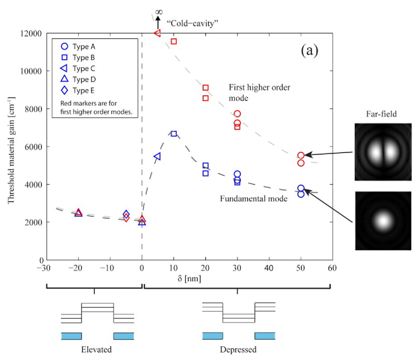  To explore the threshold gain’s dependence on the depression δ in more detail, the different contributions to the cavity loss, i.e. absorption, mirror outcoupling and lateral (diffraction and lateral leakage) loss were identified and are summarized in Fig. 10 for the fundamental mode in the cold-cavity case. The absorption and outcoupling losses do not vary much with the depression parameter δ, while the lateral loss is strongly dependent on nm-sized changes in the cavity structure. More information regarding this study can be found in Ref.132,133. Figure 10.The loss analysis including absorption, mirror outcoupling and lateral loss for different depressions δ for the fundamental mode in the cold cavity case.  To avoid optically anti-guided structures with high optical losses, i.e. structures with a depression in the center, new current and optical confinement schemes are now being developed by several groups. Cosendey and coworkers at EPFL32, have obtained transverse current confinement using reactive ion etching (RIE)-treatment to not only passivate the p-GaN surface but also etch very slightly in the periphery to form a shallow elevated structure in the center of about 10 nm. Their devices from the same epitaxial material, but with a “standard” SiO2 aperture that creates a depression in the center of the device, did not lase at all. Lai et al. at National Chiao Tung University made a shallow mesa etch in their microcavity structure and observed an improvement on optical confinement and cavity quality factor142. Leonard and coworkers at UCSB fabricated devices incorporating Al ion-implanted apertures in order to achieve a planar design without any depression or elevation in the center36. However, the built-in optical guiding was small due to the small index contrast between the implanted region and the center of the device, but anyway led to devices with a five times lower threshold current than their “standard” silicon nitride apertures. The UCSB team has also realized an airgap aperture by photoelectrochemical lateral undercut etching to selectively remove the multiple QWs outside the aperture region. This led to a strong lateral optical confinement due to the large refractive index contrast between airgap and QWs and no filamentation in the laser38. 5.TIO2/AIR HIGH CONTRAST GRATING REFLECTORS FOR GAN-BASED VCSELSFor GaN-based microcavity light emitters, such as VCSELs and resonant cavity light emitting diodes (RCLEDs) in the blue-green wavelength regime, to obtain a highly reflective feedback mirror with wide bandwidth is truly challenging. In this respect, the high contrast grating (HCG) structures have been quite popular recently as the top reflectors in VCSELs thanks to their potential advantages, over the much thicker conventional distributed Bragg reflectors (DBRs), such as broadband high reflectivity, wavelength setting capability, transverse mode control, and polarization selectivity. Very high performance HCGs have been demonstrated in different material systems such as GaAs, AlGaAs, InP, Si, etc. However much inferior performance has been achieved for GaN-based HCGs due to difficulties in this material system: there is no simple way to find a sacrificial layer with high wet etch selectivity to GaN. Attempts to realize III-nitride membrane type HCG structures for the visible regime have been limited to bandgap selective photoelectrochemical (PEC) etching of InGaN superlattices74, and focused-ion-beam (FIB) etching75, to make airgaps. We proposed a new approach to achieve HCGs for GaN-based VCSELs using dielectric materials instead82. TiO2 is a dielectric material which has a refractive index similar to that of GaN and has a very low optical absorption for wavelengths above 400 nm. Moreover, a high etch selectivity can be achieved between SiO2 and TiO2 making them very suitable to be used as the sacrificial and grating materials, respectively. Rigorous coupled-wave analysis (RCWA) simulations have been performed to design the free-standing TiO2 HCGs143. The resulting reflectance contour plots (with reflectivities above 99%) versus duty cycle and period (Λ) are shown in Fig. 11, for both the electric field perpendicular to the gratings bars (TM polarized light) and parallel to the grating bars (TE polarized light). The gratings were designed for a wavelength of 450 nm, where the refractive index of TiO2 is 2.6. As seen in the figure, for TM polarized light, the tolerance window for fabrication imperfection is larger than for TE polarized light, thus the gratings were designed to yield high reflectivity for TM polarized light. Figure 11.The reflectance contour plots (reflectivities above 99%) for TiO2/air HCG using the optimal layer thickness values for (a) TE-polarized light, TiO2 layer thickness tg = 145 nm, airgap height ha = 550 nm, and (b) TM-polarized light, tg = 205 nm, ha = 400 nm. 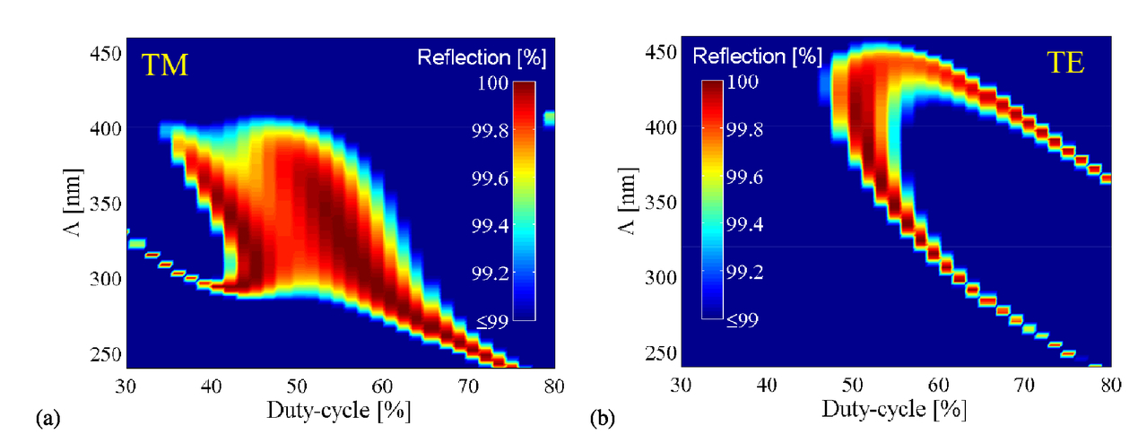 To fabricate the HCGs, a Ni/SiO2-hard mask was defined by e-beam lithography and lift-off of the Ni-layer and subsequent dry etching of the SiO2. The pattern was transferred into the TiO2 by dry etching, the Ni removed in Ni-Cr-etchant, and the sacrificial SiO2-layer was under-etched in a buffered oxide etch. Critical point drying was used to avoid stiction and collapse of the grating bars. SEM-images of the fabricated free-standing TiO2 HCG structures are shown in Fig. 12. Figure 12.SEM image of a free-standing TiO2 HCGs with a period of 350 nm and duty-cycle of about 50% in (a) top view and (b) cross-sectional view.  The fabricated HCGs were fabricated to fit onto VCSEL mesas, and therefore had a quite small diameter of less than 20μm. Therefore, a micro-reflectance measurement setup was employed for characterization. However, since the microscope objectives have a certain numerical aperture the illumination and capture angle will not only be normally incident. In the setup used, the acceptance cone included angles up to 6°. More details about the characterization method and constraints to be able to estimate the absolute reflectance of these HCG structures can be found in Ref.82. Fig. 13 contains the extracted reflectance spectra for both TM and TE polarized light. Peak reflectance values exceeding 95% near the center wavelength of 435 nm with a full-width at half-maximum (FWHM) for the stopband of about 80 nm are achieved for the TM polarized light. The peak reflectance for the TE polarized light is however only 30% lower which is a much smaller difference than the theoretical predictions indicate. This is because it is not possible to isolate the reflectivity of the HCG from that of the structure beneath. The HCG is poorly reflective for TE polarized light and therefore a large reflection comes from the air/Si substrate interface, which has been included in the simulations. To get a good agreement between measured reflectivity spectrum and simulated it is important to also consider the finite acceptance angle of 6° in the measurement set-up, which is included in the simulations by averaging the reflectance values for different angles of the incoming light. The difference between including and not including non-normally incident light in the simulations can be seen by comparing Fig. 13 (a) and (b). Figure 13.Measured reflectance spectra of the TiO2 HCG with a period of 370 nm, a duty cycle of about 45%, a grating layer thickness of 210 nm and an airgap of 340 nm, for both TM and TE polarized light, and (a) simulations assuming only normally incident light and (b) simulations accounting for a finite acceptance angle of 6°.  6.SUMMARYThe realization of electrically injected GaN-based VCSELs is challenging, but the progress in recent years is encouraging. Several groups have now demonstrated electrically pumped devices with an optical output power close to 1 mW and threshold current densities between 3-16 kA/ cm2. Some of the key challenges are to achieve high-reflectivity mirrors, vertical and lateral carrier confinement, efficient lateral current spreading, accurate cavity length control and lateral mode confinement. In this paper we have summarized state-of-the-art results and highlighted our work on combined lateral current and optical mode confinement, where we show that many structures used for current confinement result in unintentionally optically anti-guided resonators. Such resonators can have a very high optical loss, which easily doubles the threshold gain for lasing. We have also presented an alternative to distributed Bragg reflectors as high-reflectivity mirrors, namely TiO2/air high contrast gratings (HCGs). Fabricated HCGs of this type show a high reflectivity (>95%) over a 25 nm wavelength span. ACKNOWLEDGEMENTSThe authors would like to thank Henrik Frederiksen, Mats Hagberg, and Bengt Nilsson from the MC2 Nanofabrication Laboratory at Chalmers University of Technology, Sweden, for technological support in the processing, and Nicolas Grandjean and co-workers at EPFL, Switzerland for discussions on the layer structures used in GaN-VCSELs and providing the micro-reflectance measurement setup. This work was funded by the Swedish Energy Agency, Swedish Foundation for Strategic Research, and the Swedish Research Council. REFERENCESK. Iga, IEEE J. Sel. Top. Quantum Electron.,, 6
(6), 1201
–1215
(2000). https://doi.org/10.1109/2944.902168 Google Scholar
H. Soda, K. Iga, C. Kitahara, and Y. Suematsu, 18
(12), 2329
–2330
(1979). Google Scholar
I. Melngailis, Appl. Phys. Lett., 6 59
–60
(1965). https://doi.org/10.1063/1.1754164 Google Scholar
F. Koyama, S. Kinoshita, and K. Iga, Appl. Phys. Lett.,, 55
(3), 221
–222
(1989). https://doi.org/10.1063/1.101913 Google Scholar
Y. H. Lee, J. L. Jewell, A. Scherer, S. L. McCall, J. P. Harbison, and L. T. Florez, Electron. Lett.,, 25
(20), 1377
–1378
(1989). https://doi.org/10.1049/el:19890921 Google Scholar
R. Michalzik, VCSELs - Fundamentals, Technology and Applications of Vertical-Cavity Surface-Emitting Lasers, 12 Springer-Verlag Berlin Heidelberg, p.2013). Google Scholar
J. J. D. McKendry, D. Massoubre, S. Zhang, B. R. Rae, R. P. Green, E. Gu, R. K. Henderson, A. E. Kelly, and M. D. Dawson, J. Lightwave Technol., 30 61
(2012). https://doi.org/10.1109/JLT.2011.2175090 Google Scholar
J. J. D. McKendry, R. P. Green, A. E. Kelly, Z. G. Z. Gong, B. Guilhabert, D. Massoubre, E. Gu, and M. D. Dawson, IEEE Photonics Technol. Lett., 22 1346
(2010). https://doi.org/10.1109/LPT.2010.2056360 Google Scholar
C. Lee, C. Zhang, M. Cantore, R. M. Farrell, S. Ho Oh, T. Margalith, J. S. Speck, S. Nakamura, Optics Express, 23
(12), 16232
–16237
(2015). https://doi.org/10.1364/OE.23.016232 Google Scholar
Y.-C. Chi, D.-H. Hsieh, C.-T. Tsai, H.-Y. Chen, H.-C. Kuo, and G.-R. Lin, Optics Express, 23
(10), 13051
–13059
(2015). https://doi.org/10.1364/OE.23.013051 Google Scholar
L. Y. Kuritzky and J. S. Speck, MRS Communications, 5 463
–473
(2015). https://doi.org/10.1557/mrc.2015.53 Google Scholar
J. J. Wierer, and J. Y. Tsao, Phys. Status Solidi A, 212
(5), 980
–985
(2015). https://doi.org/10.1002/pssa.v212.5 Google Scholar
N. Mukoyama, H. Otoma, J. Sakurai, N. Ueki, and H. Nakayama,
in Proc. of SPIE VCSELs VII,
69080H
(2008). Google Scholar
P. Kung, M. Razeghi, Optoelectronics Review, vol., 8
(3), 201
–239
(2000). Google Scholar
R. R. Hainich, O. Bimber,
“Displays: fundamentals and applications,”
CRC Press, Taylor and Francis group, (2011). Google Scholar
A. Pruijmboom, M. Schemmann, J. Hellmig, J. Schutte, H. Moench, J. Pankert,
in Proc. of SPIE Vertical-Cavity Surface-Emitting Lasers XII,
69080I
(2008). Google Scholar
A. A. Bergh, Phys. stat. sol. (a), 201
(12), 2740
–2754
(2004). https://doi.org/10.1002/(ISSN)1521-396X Google Scholar
L.J. Walsh, Australian Dental Journal, 48
(3), 146
–155
(2003). https://doi.org/10.1111/j.1834-7819.2003.tb00025.x Google Scholar
C. Goßler, C. Bierbrauer, R. Moser, M. Kunzer, K. Holc, W. Pletschen, K. Köhler, J. Wagner, M. Schwaerzle, P. Ruther, O. Paul, J. Neef, D. Keppeler, G. Hoch, T. Moser and U. T. Schwarz, J. Phys. D: Appl. Phys., 47 205401
(2014). https://doi.org/10.1088/0022-3727/47/20/205401 Google Scholar
V. Poher, N. Grossman, G. T. Kennedy, K. Nikolic, H. X. Zhang, Z. Gong, E. M. Drakakis, E. Gu, M. D. Dawson, P. M. W. French, P. Degenaar and M. A. A. Nei, J. Phys. D: Appl. Phys., 41 094014
(2008). https://doi.org/10.1088/0022-3727/41/9/094014 Google Scholar
M. K. Hibbs-Brenner, K.L. Johnson, and M. Bendett,
in Proc. of SPIE Photons and Neurons,
(2009). Google Scholar
I. P. Clements, A. G. Gnade, A. D. Rush, C. D. Patten, M. C. Twomey, and A. V. Kravitz, 8586
(2013). Google Scholar
M. Panjehpour, C. E. Julius, M. N. Phan. T. Vo-Dinh, and S. Overholt, and N. Phan, Lasers in surgery and medicine, 31 367
–373
(2002). https://doi.org/10.1002/(ISSN)1096-9101 Google Scholar
T. Vo-Dinh, M. Panjehpour, B. F. Overholt, C. Farris, F. P. Buckley, and R. Sneed, Lasers in surgery and medicine, 16
(1), 41
–47
(1995). https://doi.org/10.1002/(ISSN)1096-9101 Google Scholar
S. P. Najda, P. Perlin, M. Leszczynski, T. Slight, W.Meredith, M.Schemmann, and H. Moseley,
in Proc. of SPIE, Imaging, Manipulation, and Analysis of Biomolecules, Cells, and Tissues XIII,
(2015). Google Scholar
M. Borowiak, W. Nahaboo, M. Reynders, K. Nekolla, P. Jalinot, J. Hasserodt, M. Rehberg, M. Delattre, S. Zahler, A. Vollmar, D. Trauner, and O. Thorn-Seshold, Cell, 162 403
–411
(2015). https://doi.org/10.1016/j.cell.2015.06.049 Google Scholar
Y. Higuchi, K. Omae, H. Matsumura, and T. Mukai, Appl. Phys. Express, 1 121102
(2008). https://doi.org/10.1143/APEX.1.121102 Google Scholar
T. Onishi, O. Imafuji, K. Nagamatsu, Y. Kawaguchi, K. Yamanaka, and S. Takigawa, IEEE J. Quant. Electron., 48
(9), 1107
(2012). https://doi.org/10.1109/JQE.2012.2203586 Google Scholar
S. Izumi, N. Fuutagawa, T. Hamaguchi, M. Murayama, M. Kuramoto, and H. Narui, Appl. Phys. Express, 8 062702
(2015). https://doi.org/10.7567/APEX.8.062702 Google Scholar
T.-C. Lu, C.-C. Kao, H.-C. Kuo, G.-S. Huang, and S.-C. Wang, Appl. Phys. Lett., 92 141102
(2008). https://doi.org/10.1063/1.2908034 Google Scholar
D. Feezell,
in Proc. of SPIE,
(2015). Google Scholar
G. Cosendey, A. Castiglia, G. Rossbach, J.-F. Carlin, and N. Grandjean, Appl. Phys. Lett., 101 15
(2012). https://doi.org/10.1063/1.4757873 Google Scholar
C. O. Holder, J. S. Speck, S. P. DenBaars, S. Nakamura, and D. Feezell, Appl. Phys. Express, 5 092104
(2012). https://doi.org/10.1143/APEX.5.092104 Google Scholar
C. Holder, D. Feezell, J. S. Speck, S. P. DenBaars, and S. Nakamura,
in Proc. of SPIE,
863906
–1
(2013). Google Scholar
C. O. Holder, J. T. Leonard, R. M. Farrell, D. A. Cohen, B. Yonkee, J. S. Speck, S. P. DenBaars, S. Nakamura, and D. F. Feezell, Appl. Phys. Lett., 105 031111
(2014). https://doi.org/10.1063/1.4890864 Google Scholar
J. T. Leonard, D. A. Cohen, B. P. Yonkee, R. M. Farrell, T. Margalith, S. Lee, S. P. DenBaars, J. S. Speck, and S. Nakamura, Appl. Phys. Lett., 107 011102
(2015). https://doi.org/10.1063/1.4926365 Google Scholar
J. T. Leonard, E. C. Young, B. P. Yonkee, D. A. Cohen, T. Margalith, S. P. DenBaars, J. S. Speck, and S. Nakamura, Appl. Phys. Lett., 107 091105
(2015). https://doi.org/10.1063/1.4929944 Google Scholar
J. T. Leonard, B. P. Yonkee, D. A. Cohen, L. Megalini, S. Lee, J. S. Speck, S. P. DenBaars, and S. Nakamura, Appl. Phys. Lett., 108 031111
(2016). https://doi.org/10.1063/1.4940380 Google Scholar
T.-C. Lu, J.-R. Chen, S.-W. Chen, H.-C. Kuo, C.-C. Kuo, C.-C. Lee, and S.-C. Wang, IEEE J. Sel. Top. Quantum Electron., 15 850
(2009). https://doi.org/10.1109/JSTQE.2009.2013181 Google Scholar
T.-C. Lu, S.-W. Chen, T.-T. Wu, P.-M. Tu, C.-K. Chen, C.-H. Chen, Z.-Y. Li, H.-C. Kuo, and S.-C. Wang, Appl. Phys. Lett., 97 071114
(2010). https://doi.org/10.1063/1.3483133 Google Scholar
T.-C. Lu, T.-T. Wu, S.-W. Chen, P.-M. Tu, Z.-Y. Li, C.-K. Chen, C.-H. Chen, H.-C. Kuo, S.-C. Wang, H.-W. Zan, and C.-Y. Chang, IEEE J. Sel. Top. Quantum Electron., 17 1594
(2011). https://doi.org/10.1109/JSTQE.2010.2045477 Google Scholar
B. C. Lin, Y. A. Chang, K. J. Chen, C. H. Chiu, Z. Y. Li,Y. P. Lan, C. C. Lin, T. Lee, Y. K. Kuo, M. H. Shih, H. C. Kuo, T. C. Lu and S. C Wang, Laser Phys. Lett., 11 085002
(2014). https://doi.org/10.1088/1612-2011/11/8/085002 Google Scholar
D. H. Hsieh, A. J. Tzou, T. S. Kao, F. I. Lai, D. W. Lin, B. C. Lin, T- C. Lu, W. C. Lai, C. H. Chen, and H. C. Kuo, Opt. Express, 23
(21), 27145
–27151
(2015). https://doi.org/10.1364/OE.23.027145 Google Scholar
K. Omae, Y. Higuchi, K. Nakagawa, H. Matsumura, and T. Mukai, Appl. Phys. Express, 2 052101
(2009). https://doi.org/10.1143/APEX.2.052101 Google Scholar
D. Kasahara, D. Morita, T. Kosugi, K. Nakagawa, J. Kawamata, Y. Higuchi, H. Matsumura, and T. Mukai, Appl. Phys. Express, 4 072103
(2011). https://doi.org/10.1143/APEX.4.072103 Google Scholar
W. Liu, X. Hu, L. Ying, J. Zhang, and B. Zhang, Appl. Phys. Lett., 104 251116
(2014). https://doi.org/10.1063/1.4885384 Google Scholar
T. Hamaguchi, N. Fuutagawa, S. Izumi, M. Murayama, and H. Narui, Phys. Status Solidi A, 1
–7
(2016). Google Scholar
P. Westbergh, J. S. Gustavsson, Å. Haglund, M. Sköld, A. Joel, and A. Larsson, IEEE J. of Sel. Top. in Quantum Electron.,, 15
(3),
(2009). https://doi.org/10.1109/JSTQE.2009.2015465 Google Scholar
P. Westbergh, J. S. Gustavsson, B. Kögel, Å. Haglund, and A. Larsson, IEEE J. of Sel. Top. in Quantum Electron.,, 17
(2011). https://doi.org/10.1109/JSTQE.2011.2114642 Google Scholar
O. Mitrofanov, S. Schmult, M. J. Manfra, T. Siegrist, N. G. Weimann, and A. M. Sergent, Appl. Phys. Lett., 88 171101
(2006). https://doi.org/10.1063/1.2195547 Google Scholar
A. Bhattacharyya, S. Iyer, E. Iliopoulos, A. V. Sampath, J. Cabalu, T. D. Moustakas, and I. Friel, J. Vac. Sci. Technol. B, 20 1229
(2002). https://doi.org/10.1116/1.1482070 Google Scholar
G. S. Huang, T. C. Lu, H. H. Yao, H. C. Kuo, S. C. Wang, C. W. Lin, and L. Chang, Appl. Phys. Lett., 88 061904
(2006). https://doi.org/10.1063/1.2172007 Google Scholar
K. E. Waldrip, J. Han, J. J. Figiel, H. Zhou, E. Makarona, and A. V. Nurmikko, Appl. Phys. Lett., 78 3205
(2001). https://doi.org/10.1063/1.1371240 Google Scholar
R. Butte, J.-F. Carlin, E. Feltin, M. Gonschorek, S. Nicolay, G. Christmann, D. Simeonov, A. Castiglia, J. Dorsaz, H. J. Buehlmann, S. Christopoulos, G. Baldassarri Höger von Högersthal, A. J. D. Grundy, M. Mosca, C. Pinquier, M. A. Py, F. Demangeot, J. Frandon, P. G. Lagoudakis, J. J. Baumberg and N. Grandjean, J. Phys. D Appl. Phys., 40 6328
(2007). https://doi.org/10.1088/0022-3727/40/20/S16 Google Scholar
C. Berger, A. Dadgar, J. Bläsing, A. Lesnik, P. Veit, G. Schmidt, T. Hempel, J. Christen, A. Krost, A. Strittmatter, J. of Crystal Growth, 414 105
–109
(2015). https://doi.org/10.1016/j.jcrysgro.2014.09.008 Google Scholar
N. Nakada, H. Ishikawa, T. Egawa, and T. Jimbo, Jpn. J. Appl. Phys., 2
(42), L144
(2003). https://doi.org/10.1143/JJAP.42.L144 Google Scholar
T. Wang,
“Chapter 5 MOCVD Growth of Nitride DBRs for Optoelectronics,”
Handbook of Optical Microcavities, Pan Stanford Publishing Pte. Ltd. 978-981-4463-25-6(2015). Google Scholar
Ž. Gačević, A. Eljarrat, F. Peiró, and E. Calleja, J. Appl. Phys., 113 183106
(2013). https://doi.org/10.1063/1.4805054 Google Scholar
X. Ni, R. Shimada, T.D. Kang, J. H. Leach, and U. Ozgur, Phys. Status Solidi A, 206 367
(2009). https://doi.org/10.1002/pssa.v206:2 Google Scholar
G. Cosendey, J.-F. Carlin, N. A. K. Kaufmann, R. Butté, and N. Grandjean, Appl. Phys. Lett., 98 181111
(2011). https://doi.org/10.1063/1.3586767 Google Scholar
M. Arita, M. Nishioka, and Y. Arakawa, Phys. Stat. Sol. (a), 194
(2), 403
–406
(2002). https://doi.org/10.1002/(ISSN)1521-396X Google Scholar
T. Ive, O. Brandt, H. Kostial, T. Hesjedal, M. Ramsteiner, and K. H. Ploog, Appl. Phys. Lett., 85 1970
(2004). https://doi.org/10.1063/1.1791738 Google Scholar
D. Massoubre, L. Wang, L. Hold, A. Fernandes, J. Chai, S. Dimitrijev, and A. Iacopi, Nature Scientific reports, 5
(17026),
(2015). Google Scholar
Ueda, T., Ishida, M., and Yuri, M., Jpn. J. Appl. Phys., 50 041001
(2011). https://doi.org/10.7567/JJAP.50.041001 Google Scholar
C. Xiong, P. R. Edwards, G. Christmann, E. Gu, M. D. Dawson, J. J. Baumberg, R. W. Martin, and I. M. Watson, Semicond. Sci. Technol., 25 032001
(2010). https://doi.org/10.1088/0268-1242/25/3/032001 Google Scholar
M. Bellanger, V. Bousquet, G. Christmann, J. Baumberg, and M. Kauer, Appl. Phys. Express, 2 121003
(2009). https://doi.org/10.1143/APEX.2.121003 Google Scholar
A. Altoukhov, J. Levrat, E. Feltin, J.-F. Carlin, A. Castiglia, R. Butté, and N. Grandjean, Appl. Phys. Lett., 95 191102
(2009). https://doi.org/10.1063/1.3259720 Google Scholar
R. Sharma, E. D. Haberer, C. Meier, E. L. Hu, and S. Nakamura, Appl. Phys. Lett., 87 051107
(2005). https://doi.org/10.1063/1.2008380 Google Scholar
Y. Zhang, S.-W. Ryu, C. Yerino, B. Leung, Q. Sun, Q. Song, H. Cao, and J. Han, Phys. Status Solidi B, 247
(7), 1713
–1716
(2010). https://doi.org/10.1002/pssb.v247:7 Google Scholar
D. Chen and J. Han, Appl. Phys. Lett., 101 221104
(2012). https://doi.org/10.1063/1.4768806 Google Scholar
C. J. Chang-Hasnain and W. Yang, Adv. Opt. Photonics, 4 379
(2012). https://doi.org/10.1364/AOP.4.000379 Google Scholar
V. Karagodsky, B. Pesala, C. Chase, W. Hofmann, F. Koyama, and C. J. Chang-Hasnain, Opt. Express, 18 694
(2010). https://doi.org/10.1364/OE.18.000694 Google Scholar
E. Haglund, J.S. Gustavsson, J. Bengtsson, Å. Haglund, A. Larsson, D. Fattal, W. Sorin, and M. Tan, Opt. Express, 24
(3), 1999
–2005
(2016). https://doi.org/10.1364/OE.24.001999 Google Scholar
J. Kim, D. U. Kim, J. Lee, H. Jeon, Y. Park, and Y. S. Choi, Appl. Phys. Lett., 95 021102
(2009). https://doi.org/10.1063/1.3168552 Google Scholar
T. T. Wu, Y. C. Syu, S. H. Wu, W. T. Chen, T. C. Lu, S. C. Wang, H. P. Chiang, and D. P. Tsai, Opt. Express, 20 20551
(2012). https://doi.org/10.1364/OE.20.020551 Google Scholar
N. V. Trivino, G. Rossbach, U. Dharanipathy, J. Levrat, A. Castiglia, J.-F. Carlin, K. A. Atlasov, R. Butté, R. Houdré and N. Grandjean, Appl. Phys. Lett., 100 071103
(2012). https://doi.org/10.1063/1.3684630 Google Scholar
Y. Wang, T. Wu, T. Tanae, H. Zhu, and K. Hane, J. Micromech. Microeng., 21 105025
(2011). https://doi.org/10.1088/0960-1317/21/10/105025 Google Scholar
Y. Wang, Z. Shi, X. Li, S. He, M. Zhang, and H. Zhu, Opt. Express, 22 667
(2014). https://doi.org/10.1364/OE.22.000667 Google Scholar
Y. Wang, T. Wu, Y. Kanamori and K. Hane, Nanoscale Research Letters, 6
(367),
(2011). Google Scholar
S. Goeman, S. Boons, B. Dhoedt, K. Vandeputte, K. Caekebeke, P. Van Daele, and R. Baets, IEEE Photonics Techn. Letters, 10
(9), 1205
–1207
(1998). https://doi.org/10.1109/68.705591 Google Scholar
J. Lee, S. Ahn, H. Chang, J. Kim, Y. Park, and H. Jeon, Opt. Express, 17 22535
(2009). https://doi.org/10.1364/OE.17.022535 Google Scholar
E. Hashemi, J. Bengtsson, J. S. Gustavsson, S. Carlsson, G. Rossbach, and Å. Haglund, J. of Vac. Sci. & Techn. B, 33 050603
(2015). https://doi.org/10.1116/1.4929416 Google Scholar
B. Galler, A. Laubsch, A. Wojcik, H. Lugauer, A. Gomez-Iglesias, M. Sabathil, and B. Hahn, Phys. Status Solidi C, 8
(7-8), 2372
(2011). https://doi.org/10.1002/pssc.v8.7/8 Google Scholar
M. Meneghini, S. Vaccari, A. Garbujo, N. Trivellin, D. Zhu, C. J. Humphreys, M. Calciati, M. Goano, F. Bertazzi, G. Ghione, E. Bellotti, G. Meneghesso, and E. Zanoni, Jpn. J. Appl. Phys., 52
(8), 08JG09
(2013). https://doi.org/10.7567/JJAP.52.08JG09 Google Scholar
F. Römer, and B. Witzigmann, Appl. Phys. Lett., 106
(2), 021107
(2015). https://doi.org/10.1063/1.4905870 Google Scholar
E. Bellotti and F. Bertazzi,
“Transport Parameters for Electrons and Holes,,”
Nitride Semiconductor Devices: Principles and Simulation (J. Piprek, ed.), Chap. 4, 69, Wiley-VCH Verlag, Weinheim,
(2007). Google Scholar
C. Ren, Mater. Sci. Tech.,
(2015). Google Scholar
S. Zhang, E. Xie, T. Yan, W. Yang, J. Herrnsdof, Z. Gong, I. M. Watson, E. Gu, M. D. Dawson, and X. Hu, J. Appl. Phys., 118
(12), 125709
(2015). https://doi.org/10.1063/1.4931575 Google Scholar
M. Calciati, M. Goano, F. Bertazzi, M. Vallone, X. Zhou, G. Ghione, M. Meneghini, G. Meneghesso, E. Zanoni, E. Bellotti, G. Verzellesi, D. Zhu, and C. Humphreys, AIP Adv., 4 067118
(2014). https://doi.org/10.1063/1.4882176 Google Scholar
L. Wang, Z. H. Zhang, and N. Wang, IEEE J. Quantum Electron., 51
(5), 1
(2015). https://doi.org/10.1109/JQE.2015.2410288 Google Scholar
Y. Kawaguchi, S.-C. Huang, R. M. Farrell, Y. Zhao, J. S. Speck, S. P. DenBaars and S. Nakamura, Appl. Phys. Express, 6
(5), 052103
(2013). https://doi.org/10.7567/APEX.6.052103 Google Scholar
S. Hafiz, F. Zhang, M. Monavarian, S. Okur, V. Avrutin, H. Morkoç, and Ü. Özgür,
in SPIE Photonics West, Light- Emitting Diodes: Materials, Proc. SPIE 9003, Devices, and Applications for Solid State Lighting XVIII,
(2014). Google Scholar
G.-B. Lin, E. F. Schubert, J. Cho, J. H. Park, and J. K. Kim, ACS Photon., 2
(8), 1013
(2015). https://doi.org/10.1021/acsphotonics.5b00305 Google Scholar
T. Hager, M. Binder, G. Brüderl, C. Eichler, A. Avramescu, T. Wurm, A. Gomez-Iglesias, B. Stojetz, S. Tautz, B. Galler, S. Gerhard, R. Zeisel, and U. Strauss, Appl. Phys. Lett., 102
(23), 231102
(2013). https://doi.org/10.1063/1.4809833 Google Scholar
M. Deppner, F. Römer, and B. Witzigmann, Phys. Status Solidi RRL, 6
(11), 418
(2012). https://doi.org/10.1002/pssr.v6.11 Google Scholar
F. Römer and B. Witzigmann, Opt. Express, 22
(S6), A1440
(2014). https://doi.org/10.1364/OE.22.0A1440 Google Scholar
T. Schulz, A. Nirschl, P. Drechsel, F. Nippert, T. Markurt, M. Albrecht, and A. Hoffmann, Appl. Phys. Lett., 105 181109
(2014). https://doi.org/10.1063/1.4901256 Google Scholar
J. Piprek, R. Farrell, S. DenBaars, and S. Nakamura, IEEE Photon. Techn. Lett.,, 18
(2006). https://doi.org/10.1109/LPT.2005.860045 Google Scholar
B. C. Lin, Y. A. Chang, K. J. Chen, C. H. Chiu, Z. Y. Li, Y. P. Lan, C. C. Lin, P. T. Lee, Y. K. Kuo, M. H. Shih, H. C. Kuo, T.-C. Lu, and S.-C. Wang, Laser Phys. Lett., 11 085002
(2014). https://doi.org/10.1088/1612-2011/11/8/085002 Google Scholar
D. H. Hsieh, A. J. Tzou, T. S. Kao, F. I. Lai, D. W. Lin, B. C. Lin, T.-C. Lu, W. C. Lai, C. H. Chen, and H. C. Kuo, Opt. Express, 23
(21), 27145
–27151
(2015). https://doi.org/10.1364/OE.23.027145 Google Scholar
A. David, M. Grundmann, J. Kaeding, N. Gardner, T. Mihopoulos, and M. Krames, Appl. Phys. Lett., 92 053502
(2008). https://doi.org/10.1063/1.2839305 Google Scholar
J. Piprek, R. K. Sink, M. A. Hansen, J. E. Bowers, and S. P. DenBaars,
in Proc. of SPIE Physics and Simulation of Optoelectronic Devices VIII,
(2000). Google Scholar
J. Piprek, What is the Problem with GaN-based VCSELs?, NUSOD(2013). Google Scholar
Y.-K. Kuo and Y.-A. Chang, IEEE J. of Quantum Electronics, 40
(5), 437
(2004). https://doi.org/10.1109/JQE.2004.826437 Google Scholar
J. Piprek, Appl. Phys. Lett., 105 011116
(2014). https://doi.org/10.1063/1.4887377 Google Scholar
Y. Kawaguchi, C. Huang, Y. Wu, Q. Yan, C. Pan, Y. Zhao, S. Tanaka, K. Fujito, D. Feezell, C. Van de Walle, S. DenBaars, and S. Nakamura, Appl. Phys. Lett., 100 231110
(2012). https://doi.org/10.1063/1.4726106 Google Scholar
W. Scheibenzuber, U. Schwarz, R. Veprek, B. Witzigman, and A. Hangleiter, Phys. Rev. B, 80 115320
(2009). https://doi.org/10.1103/PhysRevB.80.115320 Google Scholar
R. A. Arif, Y.-K. Ee, and N. Tansu, Appl. Phys. Lett., 91 091110
(2007). https://doi.org/10.1063/1.2775334 Google Scholar
C.-T. Liao, M.-C. Tsai, B.-T. Liou, S.-H. Yen, and Y.-K. Kuo, J. of Applied Physics, 108 063107
(2010). https://doi.org/10.1063/1.3471804 Google Scholar
H. Zhao, L. Guangyu, J. Zhang, J. D. Poplawsky, V. Dierolf, and N. Tansu, Opt. Express, 19
(S4), A991
–A1007
(2011). https://doi.org/10.1364/OE.19.00A991 Google Scholar
J.M. Ostermann, P. Debernardi, C. Jalics, A. Kroner, M.C. Riedl, and R. Michalzik,
in Proc. of SPIE Vertical-Cavity Surface-Emitting Lasers VIII,
201
–212
(2004). Google Scholar
Å. Haglund, J.S. Gustavsson, J. Vukusic, P. Jedrasik, A. Larsson, Electron. Lett., 41
(14), 805
–807
(2005). https://doi.org/10.1049/el:20051615 Google Scholar
E. Petrolati and A. Di Carlo, Appl. Phys. Lett., 92 151116
(2008). https://doi.org/10.1063/1.2913203 Google Scholar
J. T. Leonard, D. A. Cohen, B. P. Yonkee, R. M. Farrell, S. P. DenBaars, J. S. Speck, and S. Nakamura, J. of Appl. Phys., 118 145304
(2015). https://doi.org/10.1063/1.4931883 Google Scholar
K.-K. Kim, H. Kim, S.-N. Lee, and S. Cho, Electronic Materials Letters, 7
(2), 145
–149
(2011). https://doi.org/10.1007/s13391-011-0610-0 Google Scholar
D. L. Pulfrey, G. Parish, D. Wee, B. D. Nener, Solid-State Electronics, 49 1969
–1973
(2005). https://doi.org/10.1016/j.sse.2005.09.013 Google Scholar
S. J. Chang, C. H. Lan, J. D. Hwang, Y. C. Cheng, W. J. Lin, J. C. Lin, and H. Z. Chend, J. of the Electrochemical Society, 155
(2), H140
–H143
(2008). https://doi.org/10.1149/1.2820626 Google Scholar
T.-T. Wu, C.-C. Lin, Y.-L. Wu, C.-K. Chen, T.-C. Lu, H.-C. Kuo, and S.-C. Wang, J. of Lightwave Technology, 29
(24), 3757
–3763
(2011). https://doi.org/10.1109/JLT.2011.2172916 Google Scholar
D. Feezell, R. Farrell, M. Schmidt, H. Yamada, M. Ishida, S. DenBaars, D. Cohen, and S. Nakamura, Appl. Phys. Lett., 90 181128
(2007). https://doi.org/10.1063/1.2736478 Google Scholar
M. Stattin, C. Lockhart de la Rosa, J. Sun, A. Yurgens, and Å. Haglund, Jpn. J. Appl. Phys., 52 08JG05
(2013). https://doi.org/10.7567/JJAP.52.08JG05 Google Scholar
G. Kästle, H.-G. Boyen, A. Schröder, A. Plettl, and P. Ziemann, Physical Review B, 70 165414
(2004). https://doi.org/10.1103/PhysRevB.70.165414 Google Scholar
F. Bonaccorso, Z. Sun, T. Hasan and A. C. Ferrari, Nature Photonics, 4
(2010). https://doi.org/10.1038/nphoton.2010.186 Google Scholar
J. Sun, M. T. Cole, S. A. Ahmad, O. Backe, T. Ive, M. Löffler, N. Lindvall, E. Olsson, K. B. K. Teo, J. Liu, A. Larsson, A. Yurgens, and Å. Haglund, IEEE Transactions on Semiconductor Manufacturing, 25
(3),
(2012). https://doi.org/10.1109/TSM.2012.2198676 Google Scholar
Y. S. Kim, K. Joo, S.-K. Jerng, J. H. Lee, D. Moon, J. Kim, E. Yoon, and S.-H. Chun, ACS Nano, 8
(3), 2230
–2236
(2014). https://doi.org/10.1021/nn405477f Google Scholar
M. Ortsiefer, W. Hofmann, J. Rosskopf and M.-C. Amann,
“Chapter 10 Long-Wavelength VCSELs with Buried Tunnel Junction,”
VCSELs: Fundamental, Technology and Applications of Vertical-Cavity Surface-Emitting Lasers, 1stSpringer, Berlin, Heidelberg(2013). https://doi.org/10.1007/978-3-642-24986-0 Google Scholar
S. Krishnamoorthy, D. N. Nath, F. Akyol, P. S. Park, M. Esposto, and S. Rajan, APL, 97 203502
(2010). Google Scholar
S. Krishnamoorthy, F. Akyol, P. S. Park, and S. Rajan, Appl. Phys. Lett., 102 113503
(2013). https://doi.org/10.1063/1.4796041 Google Scholar
S. Krishnamoorthy, T. F. Kent, J. Yang, P. S. Park, R. C. Myers, and S. Rajan, Nano Lett., 13 2570
(2013). https://doi.org/10.1021/nl4006723 Google Scholar
F. Akyol, S. Krishnamoorthy, and S. Rajan, Appl. Phys. Lett., 103 081107
(2013). https://doi.org/10.1063/1.4819737 Google Scholar
M. Malinverni, D. Martin, and N. Grandjean, Appl. Phys. Lett., 107 051107
(2015). https://doi.org/10.1063/1.4928037 Google Scholar
E. C. Young, B. P. Yonkee, F. Wu, S. H. Oh, S. P. DenBaars, S. Nakamura, and J. S. Speck, Appl. Physics Express, 9 022102
(2016). https://doi.org/10.7567/APEX.9.022102 Google Scholar
E. Hashemi, J. Bengtsson, J. Gustavsson, M. Stattin, G. Cosendey, N. Grandjean, and Å. Haglund, Opt. Express, 22
(1), 411
–426
(2014). https://doi.org/10.1364/OE.22.000411 Google Scholar
E. Hashemi, J. Bengtsson, J. Gustavsson, M. Stattin, M. Glauser, G. Cosendey, N. Grandjean, M. Calciati, M. Goano, and Å. Haglund,
in Proc. SPIE, Vertical-Cavity Surface-Emitting Lasers XVIII,
90010A
(2014). Google Scholar
E. Hashemi, J. Gustavsson, J. Bengtsson, M. Stattin, G. Cosendey, N. Grandjean, and Å. Haglund, Jpn. J. Appl. Phys., 52
(8S), 08JG04
(2013). https://doi.org/10.7567/JJAP.52.08JG04 Google Scholar
M. Orenstein, E. Kapon, N. G. Stoffel, J. P. Harbison, L. T. Florez, and J. Wullert, Appl. Phys. Lett., 58 804
(1991). https://doi.org/10.1063/1.105218 Google Scholar
K. J. Knopp,, D. H. Christensen, G. V. Rhodes, J. M. Pomeroy, B. B. Goldberg, and M. Selim Ünlü, 17
(8), 1429
(1999). Google Scholar
J. Wang, M. Keever, Z.-W. Feng, T. Fanning, C. Chu, A. Sridhara, F. Hopfer, T. Sale, A.-N. Cheng, B. Shao, L. Ding, P. Wen, H.-H. Chang, C. Wang, D. C. W. Hui, and L. Giovane,
in Proc. of SPIE Vertical-Cavity Surface-Emitting Lasers XVII,
(2013). Google Scholar
A. Mutig and D. Bimberg, Advances in Optical Technologies, 2011 290508
(2011). https://doi.org/10.1155/2011/290508 Google Scholar
P. Westbergh, R. Safaisini, E. Haglund, J. S. Gustavsson, A. Larsson, M. Geen, R. Lawrence, and A. Joel, IEEE Photon. Technol. Lett.,, 25
(8), 768
–771
(2013). https://doi.org/10.1109/LPT.2013.2250946 Google Scholar
B. Witzigmann, V. Laino, M. Luisier, U. T. Schwarz, G. Feicht, W. Wegscheider, K. Engl, M. Furitsch, A. Leber, A. Lell, and V. Härle, Appl. Phys. Lett., 88 021104
(2006). https://doi.org/10.1063/1.2164907 Google Scholar
G. R. Hadley, Opt. Lett., 20
(13), 1483
–1485
(1995). https://doi.org/10.1364/OL.20.001483 Google Scholar
Y.-Y. Lai, Y.-H. Chou, Y.-S. Wu, Y.-P. Lan, T.-C. Lu and S.-C. Wang,
“Fabrication and characteristics of a GaN-based microcavity laser with shallow etched mesa,,”
Appl. Phys. Express, 7
(6), 062101
(2014). https://doi.org/10.7567/APEX.7.062101 Google Scholar
L. Zhang,
“RicWaA 1.0.2 MATLAB package,,”
(2010) http://www-personal.umich.edu/~zlei/ Google Scholar
|


