|
|
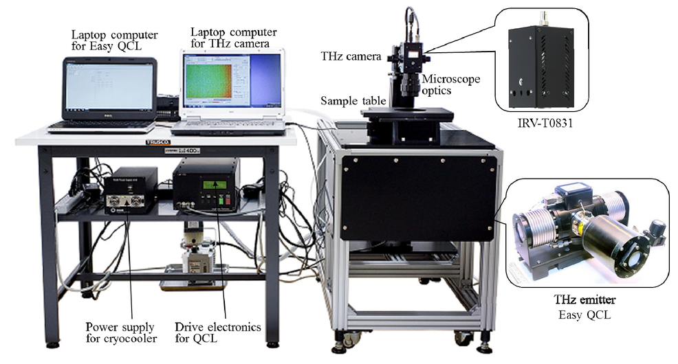
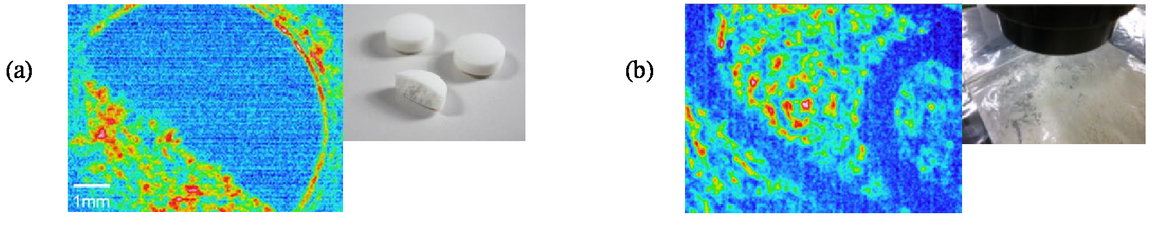
1.INTRODUCTIONTerahertz (THz) spectral region, which is also called far-infrared and/or sub-millimeter wave (sub-MMW) region, ranges from 0.1 to 10 THz. THz region has been unexplored for long time, except for astronomy, mainly due to strong water-vapor absorption in the terrestrial atmosphere, and lack of easy-to-use detectors and emitters. The calculated atmospheric transmission curves [1] indicate that THz technology is suitable for short standoff-range applications, e.g., < ca. 1 m above 1THz, > ca. 10 m below 1 THz. Since most of plastics, papers and clothes are transparent in THz region [2],[3], non-destructive inspection (NDI) is a promising application filed in industry, aerospace and military. A large number of papers have been published on THz time-domain spectroscopy (TDS). THz-TDS instruments are commercially available and used for inspecting depth profiles of tablet coating [4], depth profile of coating on a metal [5], delamination of radome [5], rust under opaque anticorrosion paint [6] and so on. In order to obtain two-dimensional or three-dimensional images with THz-TDS instrument which employs single-element detector, scanning is indispensable so that the image acquisition time becomes long. To solve this issue, real-time THz imaging over large area is requisite for many NDI applications as well as security applications, e.g., detection of concealed weapons, explosives and so on. Main components of the real-time THz imaging instrument are THz camera, THz emitter, beam homogenizer, THz optics, software for analyzing images (e.g., algorithm for detecting foreign materials). The main requisites for the instrument are compactness and price. Room temperature operation is also important to achieve cheap price. THz cameras and THz emitters have been developed and/or produced at several companies, national institutes and universities. Some THz components are commercially available, for example, THz cameras from Ophir Optronics, NEC Corporation, INO (Institut National d'Optique), TeraSense and TicWave GmbH. Market for THz camera is, for the moment, almost limited to research and development of THz emitters. In this paper, real-time cameras and detectors for THz and MMW are reviewed, which operate at room temperature. The real-time THz or MMW camera usually contains a linear array or a two-dimensional array (focal plane array (FPA)). Microbolometer (MB) THz-FPAs which are based on infrared (IR) FPA technology, have been developed since 2005 [7-10]. One of these MB-THz-FPAs (array format: 320x240, pixel pitch: 23.5 μm) covers the spectral frequency range from ca. 1 to 100 THz and is incorporated into the palm-size THz camera [11]. On the other hand, antenna-coupled CMOS (complimentary metal-oxide semiconductor) and BiCMOS (Bipolar CMOS) FPAs have been developed for detecting sub-THz radiation [12-16] and one of them (array format: 32x32, pixel pitch: 80 μm) is incorporated into a small THz camera which is sensitive to the spectral frequency range from 0.3 to 1.3 THz [17]. The III-V compound semiconductor technology also provides antenna-coupled THz arrays and imagers [18-22] as well as W-band MMW detectors and imagers [23, 24]. For example, one of imagers incorporates 8-element linear array made of GaAs Schottky diodes which detect MMW at 250 GHz in a heterodyne mode [18, 19] and another imager incorporates THz-FPA made of GaAs high-mobility heterostructure (array format: 64x64, pixel pitch: 1.5 mm), which is sensitive to the spectral frequency range from 0.05 to 0.7 THz [21,25]. The author describes development of uncooled MB-THz-FPAs, THz cameras which incorporate the MB-THz-FPAs, and active THz imaging systems. A couple of functions for the cameras are also explained, such as external-trigger imaging function and lock-in imaging function. The performances of MB-THz-FPAs are compared with those of other FPAs and detectors mentioned above. Finally, technology trend in THz and MMW emitters is briefly mentioned. 2.DEVELOPMENT OF UNCOOLED MICROBOLOMETER THZ FOCAL PLANE ARRAYSMB-THz-FPAs and THz cameras have been developed mainly at LETI (Laboratoire d'électronique des technologies de l'information), INO, NEC Corporation. The development overviews of MB-THz-FPAs at LETI and INO are described in Simoens, F. et al.[26] and Dufour, D. et al.[1], respectively. In this section, development at NEC Corporation is overviewed. Figure 1 shows the overview of development of MB-THz-FPAs carried out at NEC. First column of Fig. 1 shows schematic pixel structure of uncooled MB-IRFPA. The array format is 320x240 and pixel pitch is 23.5 μm. A thermal detector, such as a microbolometer, needs to be thermally isolated from heat sink, in this case, silicon (Si) readout integrated circuit (ROIC), to increase sensitivity. A thermal isolation structure (TIS), i.e., a suspended microbridge structure, can satisfy this condition in that it prevents the heat collected by areas sensitive to radiation from escaping to the heat sink. The pixel is divided into two parts, Si ROIC in the lower part and suspended microbridge structure in the upper part. The microbridge has a two-storied structure. The 1st floor is composed of a diaphragm and two legs, while the eaves structure is formed on the diaphragm to increase the sensitive area, or fill factor. The diaphragm and the eaves absorb IR radiation. The diaphragm is supported by the two legs so that the 1st floor is separated by air gap from Si ROIC substrate (formation of TIS). Quantum cascade laser (QCL) with an emission line at 3.1 THz was illuminated to 320x240 MB-IRFPA and minimum detectable power (MDP) per pixel was evaluated to be ca.250 pW [8]. The MDP is defined as the radiant power which produces a signal-to-noise ratio of unity in the output of a THz imager which uses a THz-FPA operating at a TV frame rate. The relation of the MDP (W) to noise-equivalent power (NEP; W/Hz0.5) is expressed by MDP=NEP/(2τint)0.5 in the case that white noise is dominant [27]. Here, τint is the integration time for the read-out electronics, presumably close to inverse of frame rate, and 1/(2τint) corresponds to the equivalent noise bandwidth. As the first improvement, THz absorption layer (thin metallic film) was added on the eaves and the diaphragm [8],[28]. The optical cavity was formed between the absorption layer and the reflection layer formed on the Si ROIC. The sheet resistance of the absorption layer was optimized for 3 THz detection (ca.30-100 Ohm). The MDP value was improved by a factor of ca. 6. Furthermore, the two-folded leg was modified to the four-folded leg, so that the diaphragm was more thermally isolated. This modification improved MDP value by a factor of ca. 1.3 [29]. As the second improvement (the rightmost column), Si cover with anti-reflection coating was put at a certain distance (half a wavelength of interest) above the eaves and the optical cavity was formed between the Si cover and the THz absorption layer [29]. This structure improved MDP value by a factor of ca. 2. It can be seen in the figure (lower right corner) that signal level of QCL beam at a location “With Si cover” is much higher than that of the beam at another location “Without Si cover”. However, this structure was not adopted as a product because of longer manufacturing process and lower yield. Figure 2 summarizes wavelength dependence of MDP for MB-THz-FPAs [11] Figure 3 shows the third improvement in the pixel structure, where a roof was added on the diaphragm. The improvement in MDP was marginal. Figure 4(a) shows the fourth improvement in the pixel structure to make MDP value better in sub-THz region [30]. A thick SiN layer (ca. 7μm thick) and a layered electrical connection were inserted between the thick metallic layer and the air-gap, so that the geometrical optical-cavity length was made much longer by a factor of three than the previous one (Fig.3). According to the calculation [30], this modification can increase sensitivity in sub-THz region, and was applied to fabrication of both 320x240 and 640x480 MB-THz-FPAs. A SEM (scanning electron microscope) picture of a part of 640x480 THz-FPA is shown in Fig.4 (b), and pictures of 640x480 and 320x240 chips are shown in Fig.4(c) and (d), respectively. Figure 4(e) summarizes spectral frequency dependences of MDP per pixel for MB-THz-FPAs. The MDP values for the fourth improvement are found better by a factor of ten in the sub-THz region than those for the third improvement [31]. 3.THZ AND SUB-THz CAMERAS3.1THz and sub-THz camerasMB-THz-FPAs mentioned above have been incorporated into a couple of THz cameras (see Fig.5). The THz camera (T0831) makes use of 320x240 MB-THz-FPA shown in Fig.3. It has a couple of functions, such as lock-in imaging, frame integration and pixel binning. The THz camera (T0832 shown in Fig.5(b)) makes use of 320x240 FPA shown in Fig.4(a) and is more sensitive to sub-THz wave than T0831 is. The 640x480 THz prototype camera was also developed (see Fig.5(c)) which contained 640x480 FPA shown in Fig.4(c). The THz camera (T0832) has the following new functions; external-trigger imaging function, beam profiling function and strip-chart-recorder function. The lock-in imaging function is also improved. Fig.5THz cameras developed by NEC Corporation. (a) 320x240 THz camera (T0831), (b) 320x240 THz camera (T0832), (c) 640x480 THz prototype camera  Other THz and sub-THz cameras are also shown in Fig.6. INO developed 384x288 MB-THz-FPA with a pixel pitch of 35 μm [32,33]. A porous gold-black film is formed on each pixel. Its thickness and porosity is ca. 50 μm and ca. 98 %, respectively, so that the effective thickness of the gold-black film is ca. 1.0 μm. The INO's camera shown in Fig.6(a) covers the spectral frequency range of 4.25-0.094THz. LETI developed antenna-coupled 320x240 MB-THz-FPA with a pixel pitch of 50 μm, which was incorporated into THz camera shown in Fig.6(b) [34,35]. For references, CMOS THz camera shown in Fig.6(c) was developed, which contained antenna-coupled 32x32 CMOS FPA (pixel pitch: 80 μm) and covered the spectral frequency range of 0.3-1.3 THz [12,17,36]. Sub-THz camera shown in Fig.6(d) was also developed, which contained 64x64 sub-THz FPA (pixel pitch: 1.5 mm) made of GaAs high-mobility heterostructure, and covered the spectral frequency range of 0.05-0.7 THz [25]. 3.2External-trigger imaging functionThe external-trigger imaging function makes use of slow thermal time constant of MB-THz-FPA which is formed on microbridge structure. The thermal time constant (τth) of the THz-FPA used in this work is ca. 19 msec [37], which is shorter than the frame time of 33 msec. The function of the external-trigger imaging was verified at 86 μm in wavelength for both 320x240 THz camera (T0832, Fig.5(b)) and 640x480 THz camera (Fig.5(c)) in combination with a pulsed THz free electron laser (THz-FEL) [38]. As to the 640x480 camera, Oda, N. et al. [39] describes the experimental results which verify correct operation of the external-trigger imaging function. Figure 7(a) shows a schematic experimental configuration of pulses for the THz camera and the THz-FEL. A brightening pulse is applied to the THz-FEL, while a trigger pulse for the THz imager is generated by a pulse generator which can shift the brightening pulse by a certain amount of time interval (ta shown in Fig.7 (b)). Figure 7(b) shows the relation of the trigger pulse for the THz imager to the brightening pulse for the THz-FEL. The repetition rate of the brightening pulse (trep) is chosen out of 2.5, 3.3, 5.0 and 10 pulses per second (pps). The trigger pulse initiates electronic scan of the THz-FPA in the THz camera. After the electronic scan is over (frame time: tfr =33 msec for the 640x480 camera, 16.7 msec for the 320x240 camera), one frame data is recorded and the THz-FPA returns to the waiting mode for the next trigger pulse coming in. In Fig.7(b), the trigger pulse TP1 initiates electronic scan of the THz-FPA in the camera. In the case of ta≪td, the pulsed THz emission ① is detected. In the case of ta≫th and tfr>td, the signal of THz-FPA for the pulsed THz emission ① almost decays, so that the pulsed THz emission ② is detected. Fig.7(a) A schematic experimental configuration of pulses for THz camera and THz-FEL, (b) Relation of the trigger pulse for the THz camera to the brightening pulse for the THz-FEL. tfr: frame time, ta + td =trep.  Figure 8(a) shows four beam patterns out of a series of ca. 110 THz pulses from THz-FEL (repetition rate: 5.0 pps, trep=200 msec) obtained with the 320x240 THz camera in the external-trigger imaging mode, where the parameter of ta=0 msec was set. The figure also shows time variation of peak signals for the THz pulses. During the measurements, the energies of the THz pulses were simultaneously measured with Joule meter, so that the normalized output signal of the THz camera was calculated in a unit of digits/μJ. The same experiments were made at the other repetition rates, so that the data plots shown in Fig.8(b) are obtained. The figure shows the consistency of the data in the repetition-rate range from 2.5 to 10 pps, considering the error bars. These experimental results verify that the function of the external-trigger imaging operates correctly for the 320x240 THz camera. The details are described in a paper presented at conference number 9856 [40]. 3.3Lock-in imaging functionLock-in imaging function was developed to increase signal-to-noise ratio (SNR) [29]. Sync signal from THz camera generated rectangular waves at such frequencies as 15, 7.5, 3.75 and 1.875 Hz (see Fig.9(a)), while QCL was driven in pulsed operation mode with a repetition frequency of 900 Hz and a pulse width of 300 ns. The pulses were applied to QCL only for the high level of the rectangular wave. THz image, i.e., “OFF image” taken during “QCL OFF” phase was subtracted from THz image, i.e., “ON image” taken during “QCL ON” phase. This function was evaluated by making QCL power very weak. It is found in Fig.9(b) that the lock-in imaging function increases SNR as a function of square root of the number of frame-integration, while frame integration without lock-in function does not so much increase SNR as expectation, because low frequency noise is predominant in microbolometer FPAs. 4.ACTIVE THZ IMAGING SYSTEMS4.1Real-Time Transmission-type Terahertz MicroscopeFigure 10 shows a picture of a transmission-type THz microscope. The microscope consists of THz emitter, illumination optics and THz camera. Easy QCL (LongWave Photonics LLC) is used as THz emitter. Frequency of emission line from QCL is 2.83 THz. The details of the microscope are described in Oda, N. et al [41]. Figures 11(a) and (b) show THz images of tablet put into an envelope and metallic clip put under flours, respectively. Tablet and clip are clearly seen. Figures 12(a) shows THz image of two sheets of 125 μm thick PVDF (Polyvinylidene difluoride) membranes prior to flowing ethanol and water. Figure 12(b) shows THz image of the PVDF membranes during flowing ethanol (upper) and water (lower). It is seen that ethanol is more transparent than water. 4.2Beam homogenizerStrong THz emitters, such as QCLs and Far infrared gas lasers, are strongly coherent and often produce interference fringes in images (e.g., see Fig.12). It is, therefore, indispensable to add beam homogenizing function to imaging system, so called, beam homogenizer. The details are described by Oda, N. et al [42]. The experimental setup shown in Fig.13(a) was assembled to investigate the fringe patterns. A THz emission line from a QCL emitter (emission frequency: 4.3 THz) illuminates an imaging area through a collimator lens and dual-axis Galvano mirrors. The Galvano mirrors wobble the THz collimated beam in horizontal and vertical directions in order to homogenize the beam. Fig.13(a) Schematic experimental setup for investigating interference fringe patterns generated by QCL, (b) THz image of sample without wobbling, (c) THz image of sample with wobbling  When the Galvano mirrors are still (no-wobbling mode), interference fringes are observed (see Fig.13(b)). The figure shows an image of two wires (ca. 300 μm in diameter) and a human hair (ca. 70 μm in diameter). When the Galvano mirrors are operated (wobbling mode), the interference fringes almost disappear (see Fig.13(c)). These experimental results show the importance of beam homogenizing function in THz imaging system which often incorporates a strong coherent THz emitter. 4.3Large-area transmission and reflection imaging system with 640x480 pixel THz camerasFigure 14 shows a large-area transmission and reflection imaging system. The details of the imaging system are described by Oda, N. et al. [30] and Ishi, T. et al. [43]. It consists of a linearly polarized THz emitter (frequency: ca.480 GHz, output power: ca.8mW), dual-axis Galvano mirrors acting as a beam homogenizer, a collimator lens, two wire-grid polarizers (WG1, WG2), a quarter-wave (QW) plate and two 640x480 THz cameras. The beam from the emitter is wobbled with the Galvano mirrors to remove interference fringes. The 480 GHz emitter has a function of a frequency modulation with a band-width of 2 GHz, which partly helps beam homogenizing. The beam from the Galvano mirrors is expanded by the collimated lens and the WG1 transmits the expanded beam. The WG2 reflects the beam which enters a sample, and the transmission image of the sample is obtained with the THz camera #1. In this case, the QW plate is moved out of optical path. Fig.14(a) Schematic diagram of the transmission and reflection imaging system, (b) the picture of the imaging system  When the reflection image of the sample is taken, the QW plate is inserted in front of the sample and the expanded beam enters the QW plate. The plate transmits the beam which is reflected back to the QW plate by the sample. Thus two passes through the QW plate rotate the direction of the linear polarization by 90 degrees and the WG2 transmits the beam which is detected with the THz camera #2. Thus, a reflection image is obtained. The cameras with the THz lenses, the wire-grid polarizers and the QW plate can be moved by using a stepping motor. This movement enables to acquire a large area THz image. The software controls the sequence of taking pictures and movement. The system is equipped with a visible camera so that an operator can know which part of the sample is imaged. The overall efficiencies of transmission and reflection imaging are 43 % and 27 %, respectively, for the optical paths from the THz emitter to the surfaces of MB-THz-FPAs. Figure 14(b) shows the picture of the imaging system. Table 1 summarizes specifications of the imaging system. Table 1Specifications of the imaging system
Figures 15(a), (b) and (c) show a visible picture of a ceramic knife (blade length: ca.23cm) put into a cardboard envelope, a 480 GHz transmission image and a 480 GHz reflection image, respectively. The imaging equipment has the feature that transmission image and reflection image of a sample are obtained by moving only the QW plate, and the reflection image is taken along the direction normal to the sample surface so that the image is not deformed. 5.COMPARISON OF PERFORMANCES FOR DIFFERENT DETECTORSIn this section, the MDP values per pixel for the MB-THz-FPAs [26,31,32,34] are compared with those of other THz detectors, such as antenna-coupled CMOS-THz-FPAs [12,13,15,16,36,44] and antenna-coupled detectors based on III-V compound semiconductor technologies [18-20,22-24]. Table 2 summarizes the parameters of these THz detectors. The MDP values for some detectors out of these detectors are estimated by Oda, N. et al [30]. Figure 16(a) shows spectral frequency dependences of the MDP values per pixel for these detectors. Above 1 THz, there is no good detector other than the MB-THz-FPAs. Simoens, F. et al [26] analyses the performance of their MB-THz-FPA and indicates that there is still a room for improvement to reach better MDP value of ca. 10 pW at 2.5 THz. In the spectral frequency range of ca. 0.3-1 THz region, the MB-THz-FPA developed at INO is more sensitive than the uncooled CMOS-THz-FPAs. Below 0.3 THz, the detectors made of III-V compound semiconductor are more sensitive than the MB-THz-FPAs and CMOS-THz-FPAs. Table 2Summary of the parameters for the THz detectors
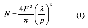
Fig.16(a) Spectral frequency dependences of the MDP values per pixel for the detectors listed in table 2, (b) spectral frequency dependences of the normalized MDP values per pixel for the detectors.  Besides the detectors listed in Table 2, Ophir Optronics’ product, Pyrocam IV [45], incorporates 320x320 pyroelectric FPA (pixel pitch: 80 μm) which covers the wide spectral-frequency range from 0.1 to 283 THz. The MDP value per pixel is 64 nW at frame rate of 25 Hz. Cox, J. A. et al. [46] developed the spiral-antenna coupled thermo-electric (TE) devices (1x8 elements) which were sensitive to the spectral-frequency range from 0.2 to 2 THz. Realization of the antenna-coupled TE-FPA operating at frame rate of 30 Hz may bring the MDP value of ca. 60 pW, using the measured NEP value of 16 pW/Hz0.5. The MB-THz-FPAs mentioned in this paper have highly-subwavelength pixel size. It is, therefore, important to propose a fair method for evaluating performances of detectors with different sizes and at different wavelengths. Normalization of MDP values to the diffraction-limited performance may be one method, which is explained as follows; the number of pixels (N) located within the FWHM (Full width at half maximum) area of the Airy disk on the focal plane is expressed by the Eq. (1). Here, F is an optics F-number, p is a pixel pitch and λ is a wavelength. Dividing the MDP values plotted in Fig. 16(a) by N0.5 provides the MDP values normalized to the diffraction-limited performance. For the normalization purpose, the F-number is set to 0.886 in this paper, which corresponds to 4F2/π=1. Figure 16(b) shows frequency dependences of the MDP values normalized to the diffraction-limited performance. Generally speaking, the normalized MDP values are better than the MDP values plotted in Fig.16(a). As to the MB-THz-FPAs, the normalized MDP values can be achieved with signal processing, such as pixel binning. 6.QUICK LOOK OF THZ AND MMW EMITTERSTechnology trend in compact and strong emitters of THz and MMW waves is briefly overviewed. DARPA has promoted several programs to develop these emitters. Figure 17 shows spectral frequency dependences of output powers from these emitters. The figure includes the results of DARPA's programs [5], the goal of Japanese program (MIC: Ministry of Internal Affairs and Communications) [47] and data for the products [43,48-50]. Below 1 THz, output powers from traveling wave tube (TWT) are much stronger than Si-based emitter and amplifier multiplier chain (AMC). In the spectral frequency range from 1.9 to 4.9 THz, QCL can emit time-average power of 5-20 mW. Combination of THz cameras with TWT or QCL may be a good choice to realize compact real-time imaging systems for applications mentioned in the introduction of this paper. Fig.17Spectral frequency dependences of output powers emitted by THz and MMW sources, where filled symbols show experimental results and/or performances described in product catalogues, while open symbol shows program goal (TWT: Traveling Wave Tube, QCL: Quantum Cascade Laser, AMC: Amplifier Multiplier Chain, MIC: Ministry of Internal Affairs and Communications, NETS: NEC Network and Sensor Systems,Ltd., LWP: LongWave Photonics LLC, VDI: Virginia Diodes Inc., HiFIVE: High Frequency Integrated Vacuum Electronics, ELASTx: Efficient Linearized All-Silicon Transmitter ICs)  7.SUMMARY AND ISSUESThe author summarizes development of uncooled MB-THz-FPAs and real-time cameras for sub-THz and THz wave detection. Active imaging systems based on the cameras are described. One of them is a real-time transmission-type THz microscope which contains a THz camera and a QCL. The other one is an active sub-THz imaging system where a transmission imaging mode and a reflection imaging mode can be switched with one-touch operation of QW plate. The performances of MB-THz-FPAs, antenna-coupled CMOS-THz-FPAs and so on, which operate at room temperature and at TV frame rate, are also summarized and compared. Technology trend in THz and MMW emitters is briefly mentioned. There are a couple of issues left for MB-THz-FPA. As pointed out by Simoens, F. et al. [26], the MDP value of ca. 10 pW can be achieved at 2.5 THz, which means that there is still a room for improvement in sensitivity by a factor of three. Nemoto, N. et al. [51] recently made measurements of polarization-dependent sensitivities of THz cameras at several spectral frequencies (0.8 to 1.9 THz). These cameras incorporate 320x240 MB-THz-FPAs (pixel pitch: 23.5 μm) and the degree of polarization is observed. Ideas for eliminating polarization-dependent sensitivity are proposed, which are composed of two patent applications and a publication of patent application [52]. Elimination of polarization-dependent sensitivity makes THz camera easier-to-use. ACKNOWLEDGMENTSThis research results have been partly achieved by the Commissioned Research of National Institute of Information and Communications Technology, and have also been partly achieved by the Cooperative Research Program of “Network Joint Research Center for Materials and Devices” (Osaka University). The author is very much grateful to Dr. A. Bergeron (INO), Dr. F. Simoens (LETI), Dr. K. Pfeiffer (TicWave GmbH) and Dr. I. Andreev (TeraSense) for permitting him to use pictures of their cameras. REFERENCESDufour, D., Marchese, L., Terroux, M., Oulachgar, H., Généreux, F., Doucet, M., Mercier, L., Tremblay, B., Alain, C., Beaupré, P., Blanchard, N., Bolduc, M., Chevalier, C., D'Amato, D., Desroches, Y., Duchesne, F., Gagnon, L., Ilias, S., Jerominek, H., Lagacé, F., Lambert, J., Lamontagne, F., Le Noc, L., Martel, A., Pancrati, O., Paultre, J-E., Pope, T., Provençal, F., Topart, P., Vachon, C., Verreault, S., Bergeron, A.,
“Review of terahertz technology development at INO,,”
J Infrared Milli Terahz Waves, 36 922
–946
(2015). https://doi.org/10.1007/s10762-015-0181-5 Google Scholar
RIKEN, NICT THz database, http://thzdb.org/RIKEN, NICT THz database, http://thzdb.org/ Dickinson, J. C., Goyette, T. M., Gatesman, A. J., Joseph, C. S., Root, Z. G., Giles, R. H., Waldman, J., and Nixon, W. E.,
“Terahertz imaging of subjects with concealed weapons,,”
in Proc. SPIE,
(2006). Google Scholar
Fitzgerald, A. J., Cole, B. E., and Taday, P. F.,
“Nondestructive Analysis of Tablet Coating Thicknesses Using Terahertz Pulsed Imaging,,”
J. Pharmaceutical Sciences, 94 177
–183
(2005). https://doi.org/10.1002/jps.20225 Google Scholar
Wallace, H. B.,
“DARPA MMW System programs and how they drive technology needs,,”
DMRC Millimeter-Wave Technology Workshop,
(2014). Google Scholar
Fuse, N., Fukuchi, T., Mizuno, M., and Fukunaga, K,
“High-speed Underfilm Corrosion Imaging using a Terahertz Camera,,”
IEEJ Transactions on Fundamentals and Materials, written in Japanese, 135 241
–246
(2015). https://doi.org/10.1541/ieejfms.135.241 Google Scholar
Peytavit, E., Agnese, P., Ouvrier Buffet, J-L., Beguin, A. and Simoens, F.,
“Room Temperature Terahertz Microbolometers,,”
in Joint 30th International Conference of Infrared and Millimeter Waves & 13th International Conference on Terahertz Electronics,
(2005). https://doi.org/10.1109/ICIMW.2005.1572506 Google Scholar
Oda, N., Yoneyama, H., Sasaki, T., Sano, M., Kurashina, S., Hosako, I., Sekine, N., Sudou, T., and Irie, T.,
“Detection of terahertz radiation from quantum cascade laser, using vanadium oxide microbolometer focal plane arrays,,”
in Proc. SPIE,
(2008). Google Scholar
Pope, T., Doucet, M., Dupont, F., Marchese, L., Tremblay, B., Baldenberger, G., Verreault, S., and Lamontagne, F.,
“Uncooled detector, optics, and camera development for THz imaging,,”
in Proc. SPIE,
(2009). Google Scholar
Simoens, F., Durand, T., Meilhan, J., Gellie, P., Maineult, W., Sirtori, C., Barbieri, S., Beere, H., and Ritchie, D.,
“Terahertz imaging with a quantum cascade laser and amorphous-silicon microbolometer array,,”
in Proc. SPIE,
(2009). Google Scholar
Oda, N., Lee, A. W. M., Ishi, T., Hosako, I., and Hu, Q.,
“Proposal for Real-Time Terahertz Imaging System, with Palm-size Terahertz Camera and Compact Quantum Cascade Laser,,”
in Proc. SPIE,
(2012). Google Scholar
Pfeiffer, U.,
“THz Imaging with Silicon-based Circuits,,”
International Workshop on Optical Terahertz Science and Technology (OTST), Tutorials for OTST, 73
–83
(2013). Google Scholar
Bauer, M., Boppel, S., Lisauskas, A., Krozer, V., and Roskos, H. G.,
“Real-time CMOS Terahertz Camera Employing Plane-to-plane Imaging With a Focal-plane Array of Field-effect Transistors,,”
in 38th International Conference of Infrared,
(2013). https://doi.org/10.1109/IRMMW-THz.2013.6665503 Google Scholar
Lisauskas, A., Boppel, S., Mundt, M., Bauer, M., Khamaisi, B., Socher, E., Seliuta, D., Minkevicius, L., Kasalynas, I., Valusis, G., Mittendorf, M., Winnerl, S., Krozer, V., and Roskos, H. G.,
“Terahertz sensing and imaging with MOSFETs from microwaves up to 9 THz,,”
Proc. European Microwave Week, 2013
(2013). Google Scholar
Kar-Roy, A., Howard, D., Preisler, E. J., and Racanelli, M.,
“Recent developments using TowerJazz SiGe BiCMOS platform for mm Wave and THz applications,,”
in Proc. SPIE,
(2013). Google Scholar
Han, R., Zhang, Y., Kim, Y., Kim, D. Y., Shichijo, H., Afshari, E., and O, K.,
“280GHz and 860GHz Image Sensors Using Schottky-Barrier Diodes in 0.μm Digital CMOS,,”
in 2012 IEEE International Solid-State Circuits Conference,
(2012). Google Scholar
TicWave GmbH, http://ticwave.com/products.html Google Scholar
Mann, C.,
“Solid State Detector Arrays for Terahertz Applications,,”
in Proc. SPIE,
(2006). Google Scholar
Mann, C., Marsh, S., Talbot, P., Slack, R., Furnace, M., Cannings, T., Green, L., Seymour, C., Hale, S., Haskett, D., Arthurs, D., and Sykes, C.,
“Towards a 0.1K delta T room temperature real time passive stand-off imager at 250GHz,,”
International Symposium on Frontiers in THz Technology (FTT 2012),
(2012). Google Scholar
Trichopoulos, G. C., Mosbacker, H. L., Burdette, D. J., and Sertel, K.,
“A Broadband Focal Plane Array Camera for Real-time THz Imaging Applications,,”
IEEE Trans. Antenna and Propagation, 61 1733
–1740
(2013). https://doi.org/10.1109/TAP.2013.2242829 Google Scholar
Muravev, V., Tsydynzhapov, G., Fortunatov, A., and Kukushkin, I.,
“High-speed THz semiconductor imaging camera,,”
in 38th International Conference of Infrared,
(2013). https://doi.org/10.1109/IRMMW-THz.2013.6665502 Google Scholar
Hesler J. L., and Crowe, T. W.,
“Responsivity and Noise Measurements of Zero-Bias Schottky Diode,,”
in 18th International Symposium on Space Terahertz Technology,
89
–92
(2007). Google Scholar
Lynch, J. J., Macdonald, P. A., Moyer, H. P., and Nagele, R. G.,
“Passive millimeter wave imaging sensors for commercial markets,,”
Applied Optics, 49 E7
–E12
(2010). https://doi.org/10.1364/AO.49.0000E7 Google Scholar
Martin, C. A., Gonzalez, C. E. G., Kolinko, V. G., and Lovberg, J. A.,
“Rapid passive MMW security screening portal,,”
in Proc. SPIE,
(2008). Google Scholar
,TeraSense, http://terasense.com/ Google Scholar
Simoens, F., Meilhan, J., and Nicholas, J-A.,
“Terahertz Real-Time Imaging Uncooled Arrays Based on Antenna-Coupled Bolometers or FET Developed at CEA-Leti,,”
J Infrared Milli Terahz Waves, 36 961
–985
(2015). https://doi.org/10.1007/s10762-015-0197-x Google Scholar
Popovic, Z., and Grossman, E. N.,
“THz Metrology and Instrumentation,,”
IEEE Trans. Terahertz Science and Technology, 1 133
–144
(2011). https://doi.org/10.1109/TTHZ.2011.2159553 Google Scholar
Oda, N.,
“Uncooled bolometer-type Terahertz focal plane array and camera for real-time imaging,,”
Comptes Rendus Physique, 11 496
–509
(2010). https://doi.org/10.1016/j.crhy.2010.05.001 Google Scholar
Oda. N., Sano. M., Sonoda, K., Yoneyama, H., Kurashina, S., Miyoshi, M., Sasaki, T., Hosako, I., Sekine, N., Sudou, T., and Ohkubo, S.,
“Development of Terahertz Focal Plane Arrays and Handy Camera,,”
in Proc. SPIE,
(2011). Google Scholar
Oda, N., Kurashina, S., Miyoshi, M., Doi, K., Ishi, T., Sudou, T., Morimoto, T., Goto, H., and Sasaki, T,
“Microbolometer Terahertz Focal Plane Array and Camera with Improved Sensitivity in the Sub-Terahertz Region,,”
J Infrared Milli Terahz Waves, 36 947
–960
(2015). https://doi.org/10.1007/s10762-015-0184-2 Google Scholar
Oda, N., Ishi, T., Kurashina, S., Sudou, T., Morimoto, T., Miyoshi, M., Doi, K., Goto, H., Sasaki, T., Isoyama, G., Kato, R., Irizawa, A., and Kawase K.,
“Performance of THz Cameras with Enhanced Sensitivity in Sub-Terahertz Region,,”
in Proc. SPIE,
(2015). Google Scholar
Mercier, L., Fisette, B., Terroux, M., Desroches, Y., Beaupré, P., Demers, M., Dufour, D., Généreux, F., Marchese, L., Topart, P., Alain, C., and Bergeron, A.,
“Wideband sensitive THz core for application integration,,”
in 40th International Conference on Infrared, Millimeter, and Terahertz Waves,
(2015). https://doi.org/10.1109/IRMMW-THz.2015.7327591 Google Scholar
Yamaguchi, Y.,
“Wideband Sensitive THz Camera Core for Application Integration,,”
in 7th TeraTech Business Seminar (THz-biz2015), written in Japanese,
(2015). Google Scholar
Meilhan, J., Simoens, F., Lalanne-Dera, J., Gidon, S., Lasfargues, G., Pocas, S., Nguyen, D.T., and Ouvrier-Buffet, J.-L.,
“Terahertz frequency agility of uncooled antenna-coupled microbolometer arrays,,”
in 37th International Conference on Infrared, Millimeter, and Terahertz Waves,
(2012). https://doi.org/10.1109/IRMMW-THz.2012.6380203 Google Scholar
Simoens, F., Meilhan, J., Lalanne-Dera, J., Gidon, S., Lasfargues, G., Martin, S., Pocas, S., Ouvrier-Buffet, J.-L., Guillaume, D., Jagtap, V., and Barbieri, S.,
“Complete THz system for reflection real-time imaging with uncooled antenna-coupled bolometer arrays,,”
in 37th International Conference on Infrared, Millimeter, and Terahertz Waves,
(2016). Google Scholar
Grzyb, J., and Pfeiffer, U.,
“THz Direct Detector and Heterodyne Receiver Arrays in Silicon Nanoscale Technologies,,”
J Infrared Milli Terahz Waves, 36 998
–1032
(2015). https://doi.org/10.1007/s10762-015-0172-6 Google Scholar
Oda, N., Okubo, S., Sudou, T., Isoyama, G., Kato, R., Irizawa, A., and Kawase, K.,
“Image Reconstruction Method For Non-Synchronous THz Signals,,”
in Proc. SPIE,
(2014). Google Scholar
Isoyama, G., Kawase, K., Irizawa, A., Kato, R., Fujimoto, M., Kamitsukasa, F., Osumi, H., Yaguchi, M., and Suga, S.,
“Terahertz Free Electron Laser at Osaka University,,”
in Proc. International Symposium on Frontiers in Terahertz Technology,
(2012). Google Scholar
Oda, N., Sudou, T., Morimoto, T., Ishi, T., Okubo, S., Isoyama, G., Irizawa, A., Kawase, K., and Kato, R.,
“Externally Triggered Terahertz Imaging For Microbolometer Focal Plane Array,,”
in 40th International Conference on Infrared, Millimeter, and Terahertz Waves,
(2015). https://doi.org/10.1109/IRMMW-THz.2015.7327705 Google Scholar
Oda, N., Sudou, T., Ishi, T., Okubo, S., Isoyama, G., Irizawa, A., Kawase, K., and Kato, R.,
“Externally Triggered Imaging Technique for Microbolometer-type Terahertz Imager,,”
in Proc. SPIE,
9856
–14
(2016). Google Scholar
Oda, N., Ishi, T., Morimoto, T., Sudou, T., Tabata, H., Kawabe, S., Fukuda, K., Lee, A. W. M., and Hu, Q.,
“Real-Time Transmission-type Terahertz Microscope, with Palm size Terahertz Camera and Compact Quantum Cascade Laser,,”
in Proc. SPIE,
(2012). Google Scholar
Oda, N., Hosako, I., Ishi, T., Minamide, H., Otani, C., and Sekine, N.,
“The Need of Terahertz Cameras for Standardizing Sensitivity Measurements,,”
J Infrared Milli Terahz Waves, 35 671
–685
(2014). https://doi.org/10.1007/s10762-014-0073-0 Google Scholar
Ishi, T., Morimoto, T., Sudou, T., and Oda, N.,
“Large-Area Transmission and Reflection Imaging with 640x480 Pixel Terahertz Camera,,”
in 40th International Conference on Infrared, Millimeter, and Terahertz Waves,
(2015). Google Scholar
Zdanevicius, J., Bauer, M., Boppel, S., Palenskis, V., Lisauskas, A., Krozer, V., and Roskos, H. G.,
“Camera for High-Speed THz Imaging,,”
J Infrared Milli Terahz Waves, 36 986
–997
(2015). https://doi.org/10.1007/s10762-015-0169-1 Google Scholar
,Ophir Optronics, http://www.ophiropt.com/ Google Scholar
Cox, J. A., Higashi, R., Nusseibeh, F., and Zins, C.,
“MEMS-based uncooled THz detectors for staring imagers,,”
in Proc. SPIE,
(2011). Google Scholar
,Ministry of Internal Affairs and Communications, http://www.soumu.go.jp/main_content/000292205.pdf Google Scholar
Masuda, N., Yoshida, M., Fujishita, Y., Kobayashi, J., Sekine, N., and Kanno, A.,
“Development of 0.1/0.3 THz-band Power Modules,,”
IEICE Technical Report, written in Japanese, ED2015-110, 111
–116
(2015). Google Scholar
,LongWave Photonics, http://www.longwavephotonics.com/ Google Scholar
Marchese, L., Terroux, M., and Bergeron, A.,
“A Compact THz imaging set-up at 750 microns,,”
in Proc. SPIE,
(2015). Google Scholar
Nemoto, N., Kanda, N., Imai, R., Konishi, K., Miyoshi, M., Kurashina, S., Sasaki, T., Oda, N., and Kuwata-Gonokami, M.,
“High-Sensitivity and Broadband, Real-Time Terahertz Camera Incorporating a Micro-Bolometer Array With Resonant Cavity Structure,,”
IEEE TRANSACTIONS ON TERAHERTZ SCIENCE AND TECHNOLOGY,
(2016). https://doi.org/10.1109/TTHZ.2015.2508010 Google Scholar
Kurashina, S., and Miyoshi, M.,
“TERAHERTZ-WAVE DETECTOR,,”
Google Scholar
|