

|
|
1.INTRODUCTIONMLEs are at the core of a multitude of advanced biophotonics systems and are supporting the rapid development of new techniques for a wide range of applications such as confocal microscopy1, flow cytometry2, genetic analysis, optogenetics3 and DNA sequencing, to name just a few. A great variety of these novel techniques rely on the enhanced specificity and resolution enabled by the laser excitation of fluorescent markers (fluorophores) and the filtered detection of their spectral response. MLEs provide a large freedom for the selection of the optimal fluorophore-excitation wavelength pair in a particular experiment, a key capability due to the fast-growing number of available markers. Moreover, the flexible inclusion of extra laser lines allows the simultaneous or sequential excitation of additional markers in the same sample. Thus, the introduction of these extra observation channels enables a precise identification of molecular or cellular subsets with a maximized information throughput. The operating wavelengths of the required lasers typically lie in the visible domain, matching the absorption spectra of the majority of the commercial fluorophores for life science applications. During the last decade, cumbersome and maintenance-intensive MLE solutions based on gas and dye lasers have been gradually replaced by compact and easy-to-use systems that rely on laser diodes and Diode-Pumped Solid State (DPSS) lasers. In these new systems, the individual lasers are typically combined and delivered via single mode and polarization maintaining output fibers. However, the combination of the individual laser beams, as well as the implementation of further functionalities, such as variable attenuation, fast external modulation (analog or digital) and switching between several output fibers are still typically performed with free space optics components such as lenses, dichroic mirrors and Acousto-Optic Modulators (AOMs). The eventual integration of these free space components into an all-in-one optoelectronic PIC can support the ongoing trend of MLE miniaturization and has the potential to further enhance the robustness of the current solutions by greatly reducing the number of optical interfaces for which accurate alignment has to be maintained. Furthermore, the large scale fabrication of application specific PICs enabled by optical lithography also promises a significant reduction of the final product cost with the replacement of expensive components such as the AOMs and the fiber switch. Last but not least, the use of PICs enables more versatile solutions that can be hardly achieved with discrete free space components. This is for example the case of the generation and fast switching of complex illumination patterns. Several PIC technology platforms such as InP and Silicon Photonics have already reached a high level of maturity with commercial deployment for optical communications applications at the near infrared (wavelengths around 1.31 µm and 1.55 µm). However, the direct application of these technologies to visible wavelengths biophotonics is usually hindered by the transparency windows of the utilized materials. This is for example the case of silicon-on-insulator based technology, since silicon becomes opaque at wavelengths below 1.1μm As an alternative, PIC technologies based on a Silicon Nitride (SiN) waveguide core and a silicon dioxide cladding offer the required transparency in a broad window, extending from 400 nm up to 2 µm4,5. Furthermore, SiN is an interesting material commonly used in CMOS electronics fabrication for passivation and masking. For integrated photonics, SiN is typically deposited using either Plasma-Enhanced Chemical Vapor Deposition (PECVD) at moderate temperatures (less than 400 °C) or Low-Pressure Chemical Vapor Deposition (LPCVD) at high temperatures (~ 800 °C). Photonic technology platforms based on LPCVD and low confinement, such as the TriPleX platform, have shown the lowest propagation loss so far (0.1 dB/cm5-7) with reported values that are competitive even when compared to traditional solutions based on silica planar waveguide circuits. On the other hand, the reduced temperature of PECVD SiN photonic circuits has been demonstrated to be very promising due to the direct compatibility with CMOS fabrication in a standard Back-End-Of-Line (BEOL) process flow9-13. Nevertheless, the mass-manufacturing compatible fabrication of LPCVD SiN PICs in the Front-End-Of-Line (FEOL) processes of a CMOS foundry has been shown to be also feasible13. We start with an analysis of the different target applications of MLEs and discuss the potential opportunities and challenges for solutions assisted by PICs (Section 2). In Section 3, we describe the general MLE architecture based on an excitation stage modified from the current commercial MLE provided by TOPTICA. In this section, we also report, based on simulations, the expected excellent light coupling into a PIC implemented in the TriPleX SiN technology. In Section 4, we describe the implementation of several integrated photonic designs including wavelength combiners, variable optical attenuators and an illumination pattern generator for flow cytometry. 2.OPPORTUNITIES AND CHALLENGES OF PICS IN MULTI-COLOR LASER ENGINES FOR BIOPHOTONICS APPLICATIONS2.1Flow CytometryModern flow cytometry allows a fast identification and separation of cells according to their size, shape or type and has become one of the most widely used techniques in life sciences14. In the typical configuration, a flow cytometer consists of a core stream of a sample solution (~20 µm diameter) containing the cells to be analyzed. A surrounding sheath fluid of saline solution (~200 µm diameter) produces a hydrodynamic focusing of the core stream and creates a flow of cells in a single line. In this configuration, the cells are interrogated one by one as they pass through a laser beam. When recording scattered and fluorescent responses simultaneously, biologists receive comprehensive and quantitative information about the examined specimen that allows precise identification and sorting. The critical requirements for the illuminating beam in flow cytometry are power stability, low noise level at high frequency and high spatial shape quality. In regards to the last point, an efficient excitation requires elliptical spots of around 60 µm in the direction perpendicular to the cell flow and 10 µm in the direction in line with the flow (see Figure 1a). The wider dimension of the elliptical beam along its major axis (60 µm) provides an almost uniform illumination field across the width of the flow (~ 20 µm) which assures that the optical response (scattering or fluorescence) does not fluctuate if cells stray from the center of the illuminating beam. On the other hand, the thinner dimension of the elliptical beam along its minor axis (10 µm) allows cells to quickly pass through the illumination point and avoids the simultaneous excitation of more than one cell at a time. Typical target cells have dimensions of 5 – 15 µm and flow in the core stream at a velocity of around 1 m/s. As cells pass through the laser beam at this speed, they generate scattering and fluorescent signals with durations in the order of several microseconds. Figure 1.Drawing of a multi-color flow cytometer and details of the required illumination pattern allowing time-domain resolution of different fluorescent signals from excited cells. b) Schematic of TOPTICA’s MLE for super-resolution applications (iChrome SLE) including several free-space optics components such as dichroics, an acousto-optic tunable filter, a fiber switch and several lenses.  Flow cytometers based on MLEs use a number of excitation wavelengths that can be focused on a single spot or at different points along the stream. The latter configuration is sometimes preferred because it enables time-domain discrimination of fluorescent signals from fluorochromes exhibiting different excitation wavelengths but similar emission spectra. As the cells go across each color beam sequentially, they emit independent pulses that can be well resolved in the time domain with a fast photodetector. In typical flow cytometers the lasers are used in Continuous Wave (CW) operation and benefit from variable optical attenuators (VOA) to adjust the excitation power for each color. In contrast to direct laser attenuation, an external VOA allows setting the laser in the optimal operating conditions, which can lead to a better performance in terms of noise and thermal stability. Flow cytometry is not very demanding in terms of power with levels of around 15 mW at the illumination point. However, in order to benefit from multi-laser excitation with separated spots, the output beams need to be very well defined in shape and spacing. In a PIC, the lithographical definition of the waveguides enables a modification of the beam shape and a very precise control of the spacing between the different colors. Furthermore, the implementation of integrated VOAs with active phase tuners allows the replacement of expensive AOMs. Thus, a MLE with PIC provides a cost effective way to control the output beam that can be refocused into the flow cell of the cytometer. 2.2Confocal Laser Scanning MicroscopyConfocal Laser Scanning Microscopy (CLSM) is a very popular technique in life sciences, semiconductor inspection and material science. In bioimaging, CLSM is commonly used in combination with fluorescence microscopy: The laser beam is raster scanned over the biological sample and the fluorescent response is recorded to create a two-dimensional image. For many applications, excitation with multiple wavelengths allows the resolution of different structures with respect to each other. This is for instance the case of the Brainbow technique for the study of neural connections that uses red, green and blue fluorescent proteins to flag individual neurons and track their pathways with distinctive colors15.For such multicolor experiments, commercial MLEs provide the combination of all wavelengths in a single output fiber. The wavelength combination is typically implemented with dichroic mirrors whose alignment needs to be very accurately maintained for an efficient coupling into the output fiber. For CLSM typical required power levels are on the order of µW for imaging and mW for bleaching. Excitation at µW levels requires the laser diodes to operate around the threshold, which leads to increased noise and stability issues when the lasers are directly modulated. Moreover, when the mirror returns to the beginning of the line (fly-back) during the raster scanning operation, a fast switching signal is typically used to blank the lasers. This blanking signal avoids an unnecessary exposure of the probe to the laser excitation and minimizes photobleaching. Other microscopy techniques that require intensity modulation and rapid switching are Controlled Light Exposure Microscopy (CLEM) and Fluorescence Recovery After Photobleaching (FRAP). The required fast switching operation is challenging, since it causes major difficulties for direct modulation as the laser does not reach thermal equilibrium. Furthermore, concomitant mode hoping between longitudinal laser modes results in spectral instability and creates artifacts in the confocal image. Additionally, CLSM usually requires particular excitation wavelengths, such as 561 nm, that are only available as DPSS lasers and therefore cannot be directly modulated at the required speeds. All these reasons make external modulation a required feature for most commercial MLE solutions targeting confocal microscopy applications. Typical implementations are based on AOMs, which are expensive components increasing the cost of the final product. Therefore, the replacement of AOMs by integrated modulators on a PIC-based solution together with the on-chip implementation of the wavelength combiner can lead to a significant cost reduction. 2.3Super-Resolution MicroscopyOn the other end of the broad spectrum of MLE applications are power intensive imaging techniques such as super-resolution microscopy. They allow imaging with a resolution higher than the diffraction limit and can be separated into two major groups: deterministic super-resolution (e.g. STED) and stochastic super-resolution (e.g. PALM, STORM). All these methods have in common that they demand relatively high excitation powers. Furthermore, in order to reach maximum efficiency, they require a few wavelengths that are often only available from DPSS but not from laser diodes. Here again, intensity modulation of these lasers requires the incorporation of external modulators. Moreover, novel illumination techniques have brought the requirement of having multiple fiber outputs. This feature requires a discrete fiber switch that is often realized with a MEMS or Galvo Scanner. All these components are expensive, add transmission losses and increase power instability due to the longer beam paths. For MLE targeting super-resolution applications, PIC technology has the potential to make additional external modulation and switching obsolete. Once the laser beams are coupled into the waveguides, these functionalities can be added in a cost-effective manner without incurring the stability problems arising as a result of direct modulation. This also allows building more compact systems than what it is possible with current mainstream technology. On the other hand, the required output power levels also represent an important challenge for PICs. All integrated components need to be designed with tight specifications in regards to allowable insertion losses. Furthermore, high power densities at required near UV wavelengths can cause long term degradation at the facets of the chips. Flexibility is also limited with PICs when a requirement of adding additional wavelengths arises after chip design and fabrication. The following table shows a summary of the different use cases: Table 1.Summary of MLE requirements for biophotonic applications.
3.DEVICE CONCEPT AND LASER-TO-CHIP COUPLINGFigure 2 shows the proposed MLE with a generic PIC. Four independent laser beams with different wavelengths are focused by lenses and coupled into the on-chip waveguides. The lasers and the PIC are integrated on a common submount that provides mechanical stability and a coarse alignment at the optical interfaces. In contrast to the common approach of coupling light into the PIC by means of the attachment of individual fibers or of an array of fibers, the proposed scheme allows tailoring the beam sizes for an optimization of the coupling efficiency at each individual wavelength. Furthermore, the complexity and cost of fiber array integration, as well as the excess losses (resulting from coupling the laser beams first into the fibers and second from the fibers into the PIC) are completely removed. Figure 2.a) Schematic diagram of the MLE with a generic PIC including integrated components such as Edge Couplers (EC), Waveguide Taps (WT), fiber Switch (SW), Variable Optical Attenuators (VOAs), Wavelength Combiners (WLC), broadband edge coupler for PIC-to-fiber coupling and Pitch Converter (PC) for applications to flow cytometers. b) Integration module with mechanical submount that assures a coarse alignment between the laser beams and the PIC input ports.  In the proposed device, TOPTICA is incorporating its COOLAC technology, which allows the automatic and accurate realignment of the beams to maximize the coupling efficiency1. In the standard configuration, all four lasers emit with linear TE polarization (in-plane with the PIC surface). However, depending on the application requirements, it is also possible to rotate the lasers in order to obtain TM (out-of-plane) polarization at the edge of the PIC. At the output of the COOLAC stage, the different laser beams are collimated and have an elliptical shape with a ratio of around 1 (in-plane):2 (out-of-plane) in the standard (TE) configuration and 2:1 in the rotated (TM) version. The state of the input polarization has important implications and can be conveniently selected in order to achieve the best PIC performance for particular applications. This is enabled by the large birefringence introduced by the waveguide geometry in TriPleX platform (single thin SiN stripe surrounded by a cladding of SiO2 7) that allows choosing between two options: First, the waveguide modes for TM polarized light are typically quite delocalized outside the waveguide core in the vertical direction. This characteristic is particularly convenient for applications that require an efficient coupling at the output of the PIC to standard single mode (SM) fibers. On the other hand, the waveguide mode profiles for TE polarized light exhibit a higher confinement in the vertical direction. This feature typically results in higher insertion losses when the waveguide modes at the PIC output are directly coupled into SM fibers. Furthermore, at lower wavelengths approaching or reaching the near-UV regime, the even higher confinement (and therefore high power density) for TE can limit the maximum operating power before resulting in facet degradation. However, TE polarization also offers some advantages: First, the effective refractive index contrast between the core and laterally surrounding cladding areas is higher for TE polarization, which allows low loss waveguide bends with smaller curvature radii than in the TM case. As a consequence, applications for TE polarization can achieve a larger density of integration for compact designs using the chip real estate more efficiently. Second, the higher confinement for TE modes also provides the freedom to set larger divergence angles in the vertical direction at the output of the PIC. As discussed below, this feature has been efficiently used to achieve the required beam pattern for application to flow cytometers in which light delivery occurs free space via beam shaping elements (lenses) at the output of the PIC. Following the light path from the lasers, the first photonic integrated components that are encountered on the chip are the edge couplers (spot size converters). These devices consist of a segment of tapered waveguide with an input width that has been optimized according to wavelength and polarization to maximize the coupling efficiency. For the proposed MLE, the collimated laser beams at the output of the COOLAC stage are focused onto the edge couplers by means of spherical lenses. Thus, the elliptical beams experience an axes inversion with final ratios of around 2:1 for TE polarization and 1:2 for TM polarization. The absolute dimensions of the beams can be rescaled by selecting the focal distance and position of the lens, trading off coupling efficiency, alignment tolerances and power handling capabilities (power densities). Figure 3a-d shows the simulated coupling efficiencies as a function of the edge coupler input width and different values of the laser beam mode field diameters (MFD) for both TE and TM polarizations. The wavelengths in the plotted examples correspond to the smallest (405 nm) and largest (640 nm) values for the target applications. For the other two relevant wavelengths (488 nm and 561 nm), the edge couplers exhibit an intermediate performance between these two extreme cases. In the simulations, the coupling efficiencies account for the mode mismatch between the waveguide mode and the laser beam. The latter has been approximated by a linearly polarized Gaussian beam. For the TE polarization, the in-plane mode field diameter (MFDi) is twice the out-of-plane mode field diameter (MFDo), whereas for the TM polarization the MFDi is half of the MFDo. In both cases, the laser beam is considered to be focused right at the beginning of the edge coupler. Figure 3.Simulated coupling efficiencies from the laser beams of TOPTICA’s commercial MLE focused onto the PIC edge by means of a spherical lens and as a function of the edge coupler width for TE polarization at a) 405 nm wavelength and b) 640 nm wavelength as well as for TM polarization at c) 405 nm and d) 640 nm. The different colors correspond to variations in the Mode Field Diameter of the focused laser beam in the direction in-plane with the surface of the PIC (MFDi) for TE polarization and the direction perpendicular to the PIC surface (MFDo) for TM polarization. Laser beams maintain their original elliptical shape since they are assumed to be focused with spherical lenses and achieve ratios of MFDi = 2xMFDo for TE polarization and MFDo = 2xMFDi for TM polarization. 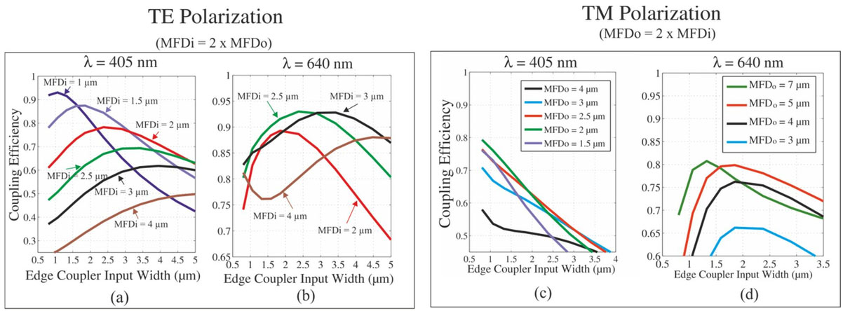 For the case of 405 nm and TE polarization (Figure 3a), corresponding to the highest confinement, it can be seen that it is possible to increase the coupling efficiency above 75% by focusing down the laser beam to a MFDi of less than 2 µm (MFDo < 1 µm) and by setting the edge coupler input width to 2 µm. However, the high mode confinement of this design can lead to degradation of the chip facet when a considerable optical power level is applied. In order to avoid this problem, it is possible to combine a larger laser beam MFDi with a larger edge coupler input width. As a drawback, this approach penalizes the coupling efficiency as the MFDo is also increased to a suboptimum value. A second solution consists in moving back the edge of the waveguide several tens of micrometers within the chip, and bridging the distance to the facet of the chip with a very wide multi-mode slab. The light can then be focused onto the edge of the waveguide inside of the chip, without exposure to atmosphere at said location. This is equivalent to what is customarily done for SM fibers at 405 nm, to which a short section of multimode fiber is added as an endcap. In this manner, the laser beam does not need to be directly focused at the chip facet and the power density at the chip-air interface can be greatly reduced. For 640 nm TE polarized light, this problem is alleviated due to the reduced confinement and it is possible to find an optimum with coupling efficiencies higher than 90% for a MFDi of around 2.75 µm (MFDo = 1.375 µm) and an edge coupler input width of 3 µm. For TM polarization (Figure 3c and d), the orientation of the elliptical axes of the rotated laser beams (ratios 1:2 with MFDi = MFDo/2) is opposed to the elliptical mode shape that naturally results from increasing the waveguide width. This limits the maximum achievable coupling efficiencies to around 80%. Furthermore, this maximum coupling efficiency can only be achieved for small values of the waveguide widths, which lead to a delocalization of the optical field outside the core and produce an almost circular shaped edge coupler mode profile. Figure 3c shows that at 405 nm the maximum coupling efficiency for a waveguide width of 1 µm can be achieved with a MFDo of 2 µm (MFDi = 1 µm). On the other hand, the maximum coupling efficiency at 640 nm is reached for a waveguide width of around 1.5 µm and a MFDo of around 6 µm (MFDi = 3 µm). Finally, it should also be noted that the coupling efficiency could be increased above 80% by means of aspherical lenses or a polarization rotation stage based on half and quarter wave plates that maintain the original elliptical orientation. Once the light beams are injected into the PIC they pass through 1% taps based on directional couplers. These components provide the feedback signal for the implementation of the control loop that allows automatic realignment with the COOLAC stage. The rest of the photonic components can be reconfigured during the design of the PIC depending on the specific application that is aimed at. As an example, in the demonstrator represented in Figure 2, a set of switches allows the selection between two different outputs: one with a pitch converter for the flow cytometer and a second one with Variable Optical Attenuators (VOAs) and a Wavelength Combiner (WC). 4.INTEGRATED PHOTONIC COMPONENTS IN SILICON NITRIDE TECHNOLOGY4.1Beam shaping for PIC-to-fiber coupler and flow cytometry illumination patternIn current commercial MLEs all combined colors are typically coupled into a single mode (SM) and polarization maintaining fiber. The implementation of a similar interface for a solution based on a PIC requires the design of an edge coupler that simultaneously adapts the output beam for each color to the respective mode profile in the SM fiber. SM fibers exhibit mode profiles with circular symmetry. Furthermore, the 1/e2 Mode Field Diameters (MFDs) in both axes typically scale with the wavelength (λ) according to the linear approximation: In the PIC, the greater refractive index contrast and the resulting greater spectral variation of modal confinement hinders the design of a device with excellent performance for all colors. Thus, it is only possible to design the output width of the edge coupler as the result of a trade-off between the coupling losses at the different wavelengths. Figure 4a shows the calculated coupling efficiencies for edge couplers with respective output widths of 0.8 and 1 µm and for both polarizations as a function of the operating wavelength. For TM polarization and 0.8 µm, the mode expands outside the waveguide core and creates a circular profile with an excellent matching to the fiber mode profile for green light. At the peak wavelength (532 nm – 580 nm) the device achieves a maximum coupling efficiency close to 90%. However, at lower (higher) wavelengths, the mode confinement increases (decreases) faster than in the fiber, which results in increased coupling losses due to mode mismatch. Nevertheless, at 405 nm and TM polarization, the PIC-to-fiber coupling efficiency is still higher than 50% Figure 4.a) Simulated PIC-to-fiber coupling efficiencies considering a standard SM fiber (MFD given by eq. 1) as a function of wavelength for edge coupler widths of 1 µm (blue) and 0.8 µm (green) and for TM polarization (solid lines) and TE polarization (dashed lines). b) Angular divergences (full angle at 1/e2 intensity) in the in-plane (solid) and out-of-plane (dashed) directions for TE polarized modes as a function of the output waveguide width. c) Ratio between in-plane and out-of-plane angular divergences as a function of the output waveguide width.  For the selected values of edge coupler output width at TE polarization, the required modal delocalization outside of the core is only reached at the longer wavelengths. As a result, the PIC-to-fiber coupling efficiency is penalized by more than 50% for wavelengths below 550 nm. On the other hand, the higher confinement of TE polarized modes makes it possible to obtain larger divergence angles in the out-of-plane direction. Figure 4b shows the calculated angular divergence in the far-field as a function of the waveguide width for the different colors. The angular divergence is defined here as a full angle and refers to the 1/e2 of the peak intensity in air. It can be seen that it is possible to reduce the divergence in the in-plane direction by increasing the waveguide width. However, in the out-of-plane direction the divergence angle increases and saturates for waveguides wider than 3 µm as a consequence of the increased confinement. For small waveguide widths, the angular divergences in both directions tend to take the same value as is expected from a beam with circular symmetry. The adjustment of the divergence angle by the definition of the waveguide width enables the implementation of an MLE output optical interface optimized for flow cytometry featuring the required beam sizes at the illumination points (60 µm by 10 µm) and a compact separation between the different colors. In the far-field, the spot size of the radiated beams (MFDλ) scales linearly with the divergence angles (θλ) and the propagation distance (z) as: In order to create the elliptical beams with the required aspect ratio, we first selected values for the waveguide widths at the PIC output facet that achieve a ratio of 6:1 between the angular divergence in the out-of-plane direction (perpendicular to the flow) and the in-plane direction (parallel to the flow). With TE polarization at all colors, these values correspond to 4.9 µm, 7.3 µm, 9.8 µm and 13 µm respectively for 405, 488, 561 and 640 nm wavelengths (marked points in Figures 4b and c). As depicted in the schematic in Figure 5a, adiabatic tapers in the in-plane direction assure the gradual conversion from the compact modes of single mode interconnection waveguides to the elliptical modes targeted at the output interface of the chip. Figure 5.a) Representation of the optical interface of a PIC generating an illumination pattern for flow cytometry. The PIC is tilted at an angle φ relative to the direction of the flow cell for compensation of the large spectral dependency of the vertical angular divergence of the emitted beams. b) MFDs (in the direction perpendicular to the PIC surface) for the different color beams as they diverge during propagation in the direction perpendicular to the cell flow. c) Normalized intensity at the illumination plane (direction parallel to the flow) of the simulated beam spots.  The large spectral dependency of the angular divergence θλ in the out-of-plane direction does not allow getting the required spot size for all colors simultaneously at a given propagation distance. For example, due to its smaller angular divergence the red beam (640 nm) needs to propagate over a larger distance than the other colors before the spot size increases to the targeted 60 µm in the out-of-plane direction. In order to compensate for the differences in divergence angles and to achieve the required spot sizes at the same illumination plane, the red color needs to begin free space propagation at a length L1 = 15.6 µm before the beam at the 561 nm wavelength. Similarly, the beam at 488 nm has to start radiating a length L2 = 14.4 µm after the beam at 561 nm. Finally, the violet beam (405 nm) has to remain guided a distance L3 = 16.3 µm longer than the blue beam (488 nm). In our design, as is illustrated in Figure 5a, the required differences in the free space optical path lengths (L1 - L3) are easily achieved by tilting the PIC at an angle φ relative to the direction of the flow and by setting the lateral separation between the waveguides at the output facet (D1 - D3) accordingly. The relation between the waveguide separation and the tilt angle can be readily calculated as: Furthermore, the tilt angle and the corresponding relative positions of the output waveguides also determine the separation between the centers of the different beams (S1-3) according to the relation: In this scheme, the waveguides reach the output facet at an angle φin that is related to the PIC tilting angle φ in air (n = 1) through the Snell’s law of refraction: with neff the effective refractive index of the modes in the SiN slab (-1.5). For the selected polarization (TE), increasing φin to the Brewster angle value (~ 34 degrees) has the benefit minimizing reflections at the PIC-air interface. However, the selection of such a steep angle also results in small values of S1-3, leading to a significant overlap (> 5%) between the adjacent beams at the illumination plane. In the flow cytometry application, a high overlap value is detrimental because it hinders the differentiation and resolution of fluorescent signals coming from adjacent spots. In our final design, the tilt angle has been fixed to φ = 39.3 degrees (φin = 25 degrees) for an overlap of less than 0.02%. Thus, the waveguides at the output facet are separated with values D1 = 24.6 µm, D2 = 22.7 µm and D3 = 25.7 µm and the laser beams at the illumination plane are separated by S1 = 19 µm, S2 = 17.6 µm and S3 = 19.9 µm, extending a total length of less than 80 µm. Figure 5c shows the normalized intensities of the different spots in the axis parallel to the flow and at the illumination plane. The slight deviations in MFDs in relation to the target value (10 µm) are derived from a near-field divergence due to the large Rayleigh range of the beams for the in-plane direction (103 µm for the beam at 640 nm) and the proximity of the projection plane (112 µm distance from the 640 nm waveguide at the PIC output facet). 4.2Variable Optical Attenuators and SwitchesIn the proposed PIC, the variable optical attenuators (VOAs) and the switches are implemented by Mach-Zehnder Interferometers (MZI). In these devices, the input light beam is equally divided in two waveguides by means of an integrated splitter (see Figure 6). The two waveguides constitute the arms of the interferometer and comprise phase tuners that allow an active adjustment of the optical phase difference (ΔΦ). At the output of the phase tuners the two light paths are again recombined and interfere in an integrated combiner. Figure 6.a) Field propagation (TM pol. Ey field amplitude) inside the 1x2 MMI designed for a wavelength of 561 nm. b) Building block diagram of the Mach-Zehnder interferometer for the implementation of the VOA and switch components. c) Field propagation (TM pol. Ey field amplitude at 561 nm) in the 2x2 MMI combiner for a phase shift difference of +90 degrees (top) and -90 degrees (bottom).  In our design, the splitter and combiner components are respectively implemented by means of 1x2 (Fig. 6a) and 2x2 (Fig. 6c) Multimode Interference couplers (MMIs). Depending on the phase difference, it is possible to adjust the power on one of the 2x2 MMI output ports (VOA functionality) or completely redirect the light beam to one port or the other (switch functionality). For the VOAs, the additional output can be used as a reference monitor for the stabilization of the power at the main port. In our demonstrator, the phase tuners leverage the thermo-optic effect in Silicon Nitride16 and are implemented by thermal resistors made of a metal layer placed above the top SiO2 cladding of the interferometer waveguides. Faster modulation speeds (in the MHz range) are also possible in TriPleX technology by means of the stress-optic effect induced by a piezoelectric lead zirconate titanate thin film17. Since the phase difference directly depends on the operating wavelength, it is necessary to implement independent VOAs and switch units optimized for every single color. In comparison with a MLE solution based on a single fiber switch, the PIC configuration allows a more versatile distribution of the laser lines between the output fibers. 4.3Wavelength CombinersThe spectral variation in modal confinement is used for the implementation of the wavelength combiner. As represented in Figure 7a, the device is comprised of three cascaded directional coupler (DC) stages. In the first DC (WLC1), the optical field at 488 nm is evanescently coupled into the adjacent bus waveguide that transports the 405 nm beam. Similarly, in the second DC (WLC2) the wave at 561 nm is coupled into the bus waveguide with the already combined waves at 405 nm and 488 nm. Finally, in a third DC (WLC3) the 640 nm light beam is also added to the other colors. The waveguide width of each DC is independently designed in such a manner that the evanescent field of the optical modes at the wavelength to be injected (higher wavelength with lower modal confinement) is significantly larger than the evanescent field at the lower wavelengths already present in the bus waveguide. Thus, by the selection of an appropriate DC gap it is possible to achieve, at the longer wavelength, a total transfer of power from one waveguide to the other, whereas only a small amount of light coupling occurs at the lower wavelengths (see Figure 7b). In a DC, the power at the output cross-port (Pcross) can be described with the expression: Figure 7.a) Schematic of the wavelength combiner based on three cascaded directional coupler stages (WLC). b) Field propagation (Ey amplitude, TM pol.) in the first WLC for the combination of the wavelengths 405 nm and 488 nm. c) Simulated transmission spectra of the different WLC in the bar port (dashed lines) and the cross port (solid lines).  with L the coupling length of the DC and Lπ,λ the half-beat length of the directional coupler. In order to achieve complete light coupling into the bus waveguide, the length of each DC is set to the half-beat length (Lλ) at the injected wavelength (longer wavelength λ).This length is adjusted in simulations to also account for the coupling that occurs in the S-bends at the input and the output of the DC. Moreover, the gap and the waveguide width are designed to be sufficiently large in order to get a Lπ,λ that is at least seven times shorter than the half-beat length for the immediately shorter wavelength(Lπ,λ=7•Lπ,λ-1). This relation assures an insertion loss of less than 5% for each of the colors already propagating in the bus waveguide. Figure 7c shows the simulated spectral response of each WLC corresponding to the cross-port (solid line) and the bar-port (dashed lines). 5.CONCLUSIONSIn this work, we have discussed a novel Multi-color Laser Engine architecture with a Photonic Integrated Circuit in Silicon Nitride (TriPleX) technology for biophotonic applications. In the proposed scheme, four wavelengths in the visible regime (405nm, 488nm, 561nm, 640nm) are free-space coupled into the PIC with an excitation stage based on a modification of the current MLE solutions commercialized by TOPTICA. Coupling efficiencies higher than 80% are possible for all four wavelengths by focusing the laser beams onto edge couplers with optimized designs. Once in the PIC, the light can be redirected and shaped to a desired output pattern and pitch, reducing the need for additional discrete optical components. We have presented PIC optical interfaces for coupling into a SM fiber and for generating an illumination pattern optimized for flow cytometry. We have also presented the design of active components such as Variable Optical Attenuators and fiber switches. These building blocks are based on Mach-Zehnder Interferometers and are assisted by thermal phase shifters. Finally, we have also presented the design of an efficient wavelength combiner based on Directional Couplers that leverages the spectral dependency of the modal confinement in TriPleX technology. ACKNOWLEDGEMENTSThis work was supported by the European Union’s Horizon 2020 research and innovation program under grant agreement no. 688519 (PIX4life). REFERENCESM. Lang,
“Lasers for Confocal Microscopy: All Colors of the Rainbow,”
Imaging & Microscopy, 2
(2011). Google Scholar
S. P. Perfetto, P. K. Chattopadhyay, and M. Roederer,
“Seventeen-colour flow cytometry: unravelling the immune system,”
Nature Reviews Immunology, 4
(8), 648
–655
(2004). https://doi.org/10.1038/nri1416 Google Scholar
K. Kampasi, E. Stark, J. Seymour, K. Na, H. G. Winful, G. Buzsáki, K. D. Wise, and E. Yoon,
“Fiberless multicolor neural optoelectrode for in vivo circuit analysis,”
Scientific Reports, 6
(2016). https://doi.org/10.1038/srep30961 Google Scholar
D. Geuzebroek, R. Dekker, E. Klein, and J. van Kerkhof,
“Photonic integrated circuits for visible light and near infrared: controlling transport and properties of light,”
Sensors and Actuators B: Chemical, 223 952
–956
(2016). https://doi.org/10.1016/j.snb.2015.09.096 Google Scholar
K. Wörhoff, R. G. Heideman, A. Leinse, and M. Hoekman,
“TriPleX: a versatile dielectric photonic platform,”
Advanced Optical Technologies, 4
(2), 189
–207
(2015). https://doi.org/10.1515/aot-2015-0016 Google Scholar
A. Leinse, R. Heideman, M. Hoekman, F. Schreuder, F. Falke, C. Roeloffzen, L. Zhuang, M. Burla, D. Marpaung, D. Geuzebroek, and R. Dekker,
“TriPleX waveguide platform: low-loss technology over a wide wavelength range,”
in in SPIE Microtechnologies. International Society for Optics and Photonics,
87670E-87670E
(2013). Google Scholar
J. F. Bauters, M. J. Heck, D. John, D. Dai, M. C. Tien, J. S. Barton, A. Leinse, R. G. Heideman, D. J. Blumenthal, and J. E. Bowers,
“Ultra-low-loss high-aspect-ratio Si3N4 waveguides,”
Optics Express, 19
(4), 3163
–3174
(2011). https://doi.org/10.1364/OE.19.003163 Google Scholar
D. Duval, J. Osmond, S. Dante, C. Domínguez, and L. M. Lechuga,
“Grating couplers integrated on Mach-Zehnder interferometric biosensors operating in the visible range,”
IEEE Photonics Journal, 5
(2), 3700108
–3700108
(2013). https://doi.org/10.1109/JPHOT.2013.2251873 Google Scholar
J. S. Levy, A. Gondarenko, M. A. Foster, A. C. Turner-Foster, A. L. Gaeta, M. Lipson,
“CMOS-compatible multiple-wavelength oscillator for on-chip optical interconnects,”
Nature Photonics, 4 37
–40
(2010). https://doi.org/10.1038/nphoton.2009.259 Google Scholar
S. Romero-García, F. Merget, F. Zhong, H. Finkelstein, and J. Witzens,
“Silicon nitride CMOS-compatible platform for integrated photonics applications at visible wavelengths,”
Optics Express, 21
(12), 14036
–14046
(2013). https://doi.org/10.1364/OE.21.014036 Google Scholar
S. Romero-García, F. Merget, F. Zhong, H. Finkelstein, and J. Witzens,
“Silicon nitride back-end optics for biosensor applications,”
in In SPIE Optics+ Optoelectronics,
87810W-87810W
(2013). Google Scholar
A.Z. Subramanian, P. Neutens, A. Dhakal, R. Jansen, T. Claes, X. Rottenberg, F. Peyskens, S. Selvaraja, P. Helin, B. Du Bois, and K. Leyssens,
“Low-loss singlemode PECVD silicon nitride photonic wire waveguides for 532-900 nm wavelength window fabricated within a CMOS pilot line,”
IEEE Photonics Journal, 5
(6), 2202809
(2013). https://doi.org/10.1109/JPHOT.2013.2292698 Google Scholar
W. D. Sacher, Y. Huang, G. Q. Lo, and J. K. Poon,
“Multilayer silicon nitride-on-silicon integrated photonic platforms and devices,”
Journal of Lightwave Technology, 33
(4), 901
–910
(2015). https://doi.org/10.1109/JLT.2015.2392784 Google Scholar
M. G. Macey,
“Flow Cytometry,”
Humana Press Incorporated,
(2007). Google Scholar
J. W. Lichtman, J. Livet, and J. R. Sanes,
“A technicolour approach to the connectome,”
Nature Reviews Neuroscience, 9
(6), 417
–422
(2008). https://doi.org/10.1038/nrn2391 Google Scholar
D. Pérez, J. Fernández, R. Baños, J. D. Doménech, A. M. sánchez, J. M. Cirera, R. Mas, J. Sánchez, S. Durán, E. Pardo, C. Domínguez, D. Pastor, J. Capmany, and P. Muñoz,
“Thermal tuners on a Silicon Nitride platform,”
arXiv preprint arXiv:1604.02958,
(2016). Google Scholar
N. Hosseini, R. Dekker, M. Hoekman, M. Dekkers, J. Bos, A. Leinse, and R. Heideman,
“Stress-optic modulator in TriPleX platform using a piezoelectric lead zirconate titanate (PZT) thin film,”
Optics Express, 23
(11), 14018
–14026
(2015). https://doi.org/10.1364/OE.23.014018 Google Scholar
|


