|
|
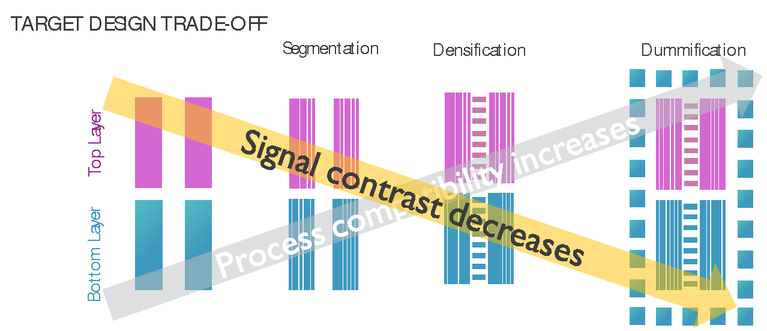
1.INTRODUCTION: METROLOGY FOR MANUFACTURING IN MULTI PATTERNING TIMEThe future development of silicon manufacturing beyond the usual scaling of dimensions implies the introduction of new material but also the increase of process complexity and the 3D architecture. It means that metrology will need to enable the extraction of profile information, allow the increase sampling and hotspot detection. This metrology will need to perform well. Total Measurement Uncertainty (TMU) and Movement Acquisition Measurement (MAM) will be key parameters driven by tool suppliers. But above all, in-line metrology must enable process control. To do so, the most important is measurement consistency, which means be process-robust to allow the reduction of metrology uncertainty. This is true for CD and Overlay metrology, but this paper will focus on overlay. In the table 1 below, we show the imec view of the required specification for the coming nodes. Different patterning options are considered. In red, the numbers are identified to be challenging, both from patterning and metrology side. Table 1.Overview of the specification to be achieved in the coming nodes (numbers in red are challenging). The metrology contribution for overlay is becoming more and more challenging as we reach the angstrom for the future nodes. Scanner capability is of course the second budget for overlay control. These two first items are integrated in the roadmap of our tool suppliers and it will not be extensively discussed here. In comparison the process contribution is a significant contributor of overlay budget (table 1). The numbers are indicative as the number of patterning option is large. The metrology challenge to enable control is to identify these process contributors. First, we need to identify the real overlay part from the damaged target which creates overlay artefact. Second, we need to improve target design to minimize process artefacts on overlay targets. 2.OVERVIEW OF EXISTING TECHNIQUES FOR OVERLAY METROLOGYImage based overlay (IBO) uses a standard optical microscopy systems using white light (or a subset of it called filter or color) while auto-focus is performed via the interferometer. The illumination in the Bright Field microscope is directed through the optical system. The targets to be measured per layers are not placed on top of each other. Each of this structure is symmetric with respect to 90° rotation. This grating target is characterized by periodic series of lines and spaces. The center of inner and outer structures is found with kernel (boxes to check the grating profile, see figure 1). The overlay is the vector between the two centers [2]. Diffraction Based Overlay (DBO) is based on an angle resolved scatterometry hardware. In angle resolved scatterometry, the illumination branch irradiates the overlay target over a large band of incidence space. The diffracted light from the grating is then captured (see figure 3). As we can see in this figure (figure2), zero order intensity varies symmetrically as a function of overlay whereas the +/-1 order intensities vary asymmetrically as a function of overlay. To define the overlay we will use the difference of intensity of the first orders [3,4,5]. Figure 3.Zero order intensity varies symmetrically as a function of overlay whereas the +/-1 order intensities vary asymmetrically as a function of overlay. To define the overlay we will use the difference of intensity of the first orders.  This asymmetry, named “As”, is function of the first order intensities: for small overlay the measured asymmetry is linearly proportional to overlay: As=K*overlay, where K is the slope of the graph figure 3.The difference of intensity of the first orders is linearly proportional to overlay. Note that in DBO targets, the 2 layers are on top of each other [6]. Finally, SEM technology interest has recently increased. This technology is capable of measuring in device but the standard CDSEM capabilities (<5 keV) need to measure once both layers are visible (figure 4). Recently new hardware has been developed to allow measurements through layers by using higher voltage SEM [7]. Figure 4.Difference signal is used to extract overlay as we assume that in a certain range, overlay response is linear.  Figure 4.Overlay SEM targets measurable with standard CDSEM (<5 kEV) on the right or advanced Overlay SEM (>5 keV) on the right.  Overlay can be extracted by a simple pitch measurement as shown in figure 5. Assuming a line of 32 nm and a CD variation of x nm for the 1st layer and y nm for the second layer, it is easy to demonstrate that overlay is not line CD dependent. In the following equation OVL is the overlay between the 2 layers. Figure 5.In a double layer illustrated by the lines 1 and 2. Assuming a CD variation of x nm for line 1 and y nm for line 2 and OVL as the overlay between the 2 layers. Overlay can be extracted from a simple measurements of the pairs d1 and d4 (or d3 and d2) [8].  In summary the table 2 shows the different target type available today. The feature width column define the typical dimension of the structure used to determine overlay by the hardware. Area defines the space occupied on the wafer. The first row shows the standard IBO targets that are used since 20 years for BiB and AIM. Then come Blossom and multi-layer AIMid which are more recent (10 years). But despite space and measurement speed advantages, they might suffer of design rule compatibility to be adopted (their segmentation is quickly impacting the performance). The DBO technology is using small recent targets (5 years) for in-die measurements. Finally SEM targets have the smallest footprint and will provide structure at design rules. Table 2.Different Overlay metrology target type. 3.DOMINANT OVERLAY ERRORS – REAL AND ARTIFACTSThe overlay errors are due to multiple process factors, the scanner being only one of them. If overlay issues reveals at lithography steps, most of the source of overlay is not lithography related. Design rule compliance for overlay target is a concern (CMP, etch, aberration effects) [9]. The target design has evolved to ensure the behavior as the device. Unfortunately, this trend is decreasing the contrast of the target (figure 6). Recently, SAxP, EUV litho or high aspect ratio processes have increased the contrast challenges. The segmentation imposed by SAxP, the thin resist thickness left after EUV litho or the increased stack thickness due to 3D processes have decreased significantly the contrast. This lack of contrast can be compensated by hardware improvement and increasing the number of filters/colors/wavelengths. In figure 7 and 8, we show 2 examples of marks damaged by process. In figure 7, the CMP process is degrading the targets in some area where CMP is sub-optimal. As the fingerprint shows, the overlay numbers are not strongly out of spec, but optical image clearly shows the damage on the target. Figure 7.CMP damage of targets in a metal process. Overlay targets are capable of compensate some minor contrast changes but when CMP is suboptimal (bottom left), the overlay signal is distorted.  Figure 8.Residual fingerprint of EUV Block on SAQP process after lithography on the left and after etch on the right. After lithography the noise is very high, but after etch the signal is back to normal. But, the correctables deduced are responding correctly even after lithography which demonstrate that this is only due to metrology noise.  In figure 8, the residual fingerprint after lithography is very high. After etch this fingerprint is back to normal. It demonstrates that the target design is good, but the signal strength is too low after lithography and creates a high random fingerprint (residual). This is the combination of the segmentation of the bottom layer due to SAQP process, plus the thickness of EUV resist for the top layer (18 nm). But the linear correctables trend through batch, before and after correction, show that measurements after litho and after etch are describing correctly the trends. It demonstrates that the problem is purely due to a metrology issue. It can be noted, to the contrary, that any nonlinear correction would have been wrong as they would be severely impacted by the noisy fingerprint. The figure 9 shows the etch impact on DBO targets (the same can be shown for IBO [10]). To demonstrate it, we changed the design in three different ways. The change of the top layer in lithography has no impact. Comparing line on line versus line on space, we can immediately see an impact of 0.005 nm/mm of grid scaling difference. Finally the change of bottom layer duty cycle design shows also an impact on grid linear scaling of the same magnitude (0.005 nm/mm). The impacts on the other correctable is minimal (not shown here). It demonstrates that the etched bottom layer is distorted and provide different answers depending on how the target is designed. This effect is not new and was already flagged years ago [10]. The effect is maximum 1 nm at the edge of the wafer, if it could be neglected in the past, due to current needs, this is becoming a problem. Figure 9.DBO target design has a strong impact on grid scaling determination for etch effect. Line on Line varying top design (left), Line on space varying top layer (middle) Line on Space varying bottom layer (right).  The different designed targets are describing different wafer signature (radial) due to etch effect. This is unsatisfying from a metrology point of view but not necessarily from a process control point of view. The figure 10 shows that these differences are only an offset. If we dial back a unique linear grid scaling correction, all targets respond correctly and describe the same correction applied (0.35 nm/mm in this case). Figure 10.All targets (DBO and IBO) respond correctly to a scaling overlay correction, independently of their offsets before correction. 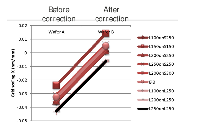 Despite the design improvements possible, the examples before show that the process effects cannot be completely eliminated. To detect these effects, the use of simultaneous targets have shown efficiency. The simultaneous target is a design composed of simultaneously both layers in one exposure. Both parts of the targets do not have the same segmentation to demonstrate the pitch dependency to process. By design, both parts, representing both layers, do not have any designed overlay. So, after lithography the overlay measured is 0 (as shown in figure 11), the 3σ numbers reflect only the pure metrology performance. But after etch or CMP, an overlay fingerprint is measured. This demonstrate that process, etch and CMP in this case, is distorting the target according to segmentation. Figure 11.Simultaneous targets can demonstrate the process distorting marks according to segmentation. In this graph the outer part of the target is not segmented and the inner part is segmented with a pitch 400 nm. 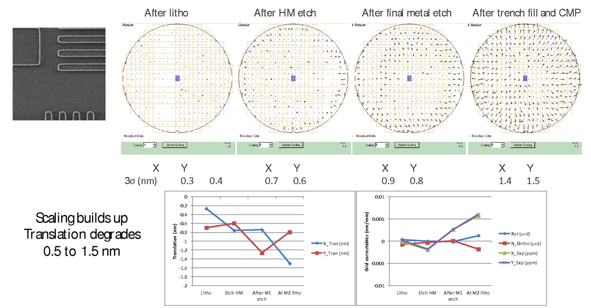 We have shown that for CMP, segmentation and dummies need optimization to balance contrast and performance. For the SAxP processes, segmentation has a preferred orientation and limited flexibility. Contrast remains a challenge, which becomes worst if block on top is EUV. Process control might impose to measure after block etch. Etch process distorts the bottom layer (feature size and tonality dependent). It creates error on grid scaling, translation, but control is maintained as offsets remains constant. Stress, warping and annealing are a challenge for control but it is not a metrology issue. In figure 12, we show an exhaustive list of all the possible sources. They are divided in 2 categories. Those that are creating a real overlay shift and those that distort the overlay target. Figure 12.Comparison of different overlay fingerprints and their cause. Some are creating a real overlay issues, some are artefacts due to damage of the overlay targets. 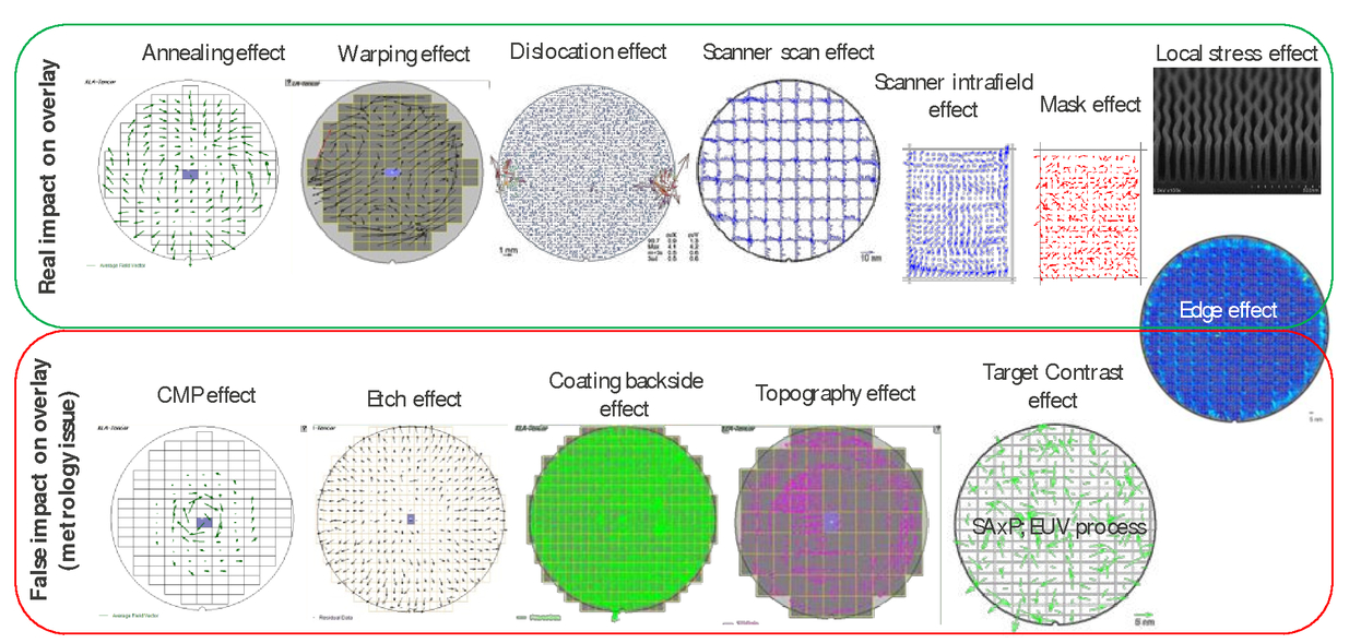 The real effects are the annealing, warping and dislocation effects. They are wafer deformation due to a specific process (annealing, oven, tensile deposition, etc…) [11]. The scan, intrafield effects are scanner related due to respectively the dynamic of the stage and the aberration of the lens and/or lens heating [12]. Mask effect is due to the registration error [23,24] when a mask is patterned, or to be correct, this is due to the mask registration difference between 2 masks that matters. Finally the local stress [13] is due to tensile material which is relaxing after patterning, this effect is real but not visible with traditional overlay technique, but even worse, can impact the overlay metrology capabilities. The false effects are a problem and must be identified because they must not be corrected. In this second part CMP, etch and contrast effects are identified through optical image of the targets showing the issue [14,15]. Concerning backside coating and topography effects, those false are identified through reference metrology [16]. Finally the edge effect is placed in between real/false because we have evidence that targets can be damaged at the edge of the wafer (coating, etch ring, etc…), but we also know through independent measurements, that edge control is a challenge for overlay. The last effect not mentioned in figure 12 cannot be clearly classified, but if it generates overlay, designing an IBO or DBO target able to detect it will be very challenging. The figure 13 shows 2 SRAM like clips after final etch in TiN. These structures are created after a triple litho-etch process. The 2 clips are pictured after etch on the same wafer at a distance of 50 um. The structure on the left shows the small horizontal trenches aligned as designed. The SRAM clip on the left shows a strong misalignment between trenches coming from 2 lithos. The difference is in the design: The left SRAM is providing a symmetric (up and down) environment to the small trenches, the right one is very asymmetric. The design asymmetry has an impact on the litho profile as seen on the left XSEM picture: Straight when dense and sloped when isolated. Figure 13.SRAM structures after final etch after a triple litho-etch process. The design symmetry of the environment creates a displacement of structures after etch.  In this chapter, we have listed the process effects that impact overlay or that impacts our target. Simultaneous marks allow the exploration of the best segmentation through any process, but it is not very cost effective, what are the alternatives? 4.SIMULATION AND TOOLING TO IMPROVE TARGET ROBUSTNESS TO PROCESSTool suppliers have provided two ways to manage the process sensitivity of targets and avoid undesired overlay artefacts. Simulation software have been developed to simulate the response of target design: MTD from KLA-Tencor [17]; D4C from ASML [18, 19]. These two software are following the same principles that is summarized in the figure 14. D4C software from ASML checks DBO target printability in lithography and detectability by YieldStar. It looks for the design which will be the less sensitive to process robustness and finally verify that lens aberrations will displace the target the same way it will for the device. On the tools themselves, target evaluation parameters have been implemented like QMerit as shown in figure 15 to allow auto-calibration of the target to minimize process sensitivity. Several algorithms are used with the same measured signal to evaluate the overlay. All the algorithms are guaranteed to give the same overlay estimate if the signal is perfectly symmetric. If the signal is not symmetric, each algorithm gives a different value. The quality metric is related to the width of the distribution of these overlay values [17]. Similar concepts are used for DBO targets where wavelength to wavelength consistency is the parameter to validate the robustness and the process consistency of a target. Figure 15.An illustration of the concept of measurement quality metric comparing different recipes using different settings [20].  But these tools are not enough as shown in figure 16. This graph shows the overlay values predicted by simulation on a given stack. The top graphs shows that in 4 wavelengths (3 of them close of the one used by the tool), the overlay numbers are out of control (resonance regime). Small process variation displace the peak but the unstable region remained centered around the same wavelength. A user would like to use the flat wavelength range to operate to guarantee that despite process variation, overlay numbers remain stable. There are three stable region. The bottom graph is complementary, by indicating the best region of the three (green arrow) to maximize the robustness of the target towards process variation. This picture demonstrates that the single wavelengths used in the tool could be insufficient, as simulation predicts that resonance peaks of the overlay signal can appear for the same few wavelengths available on the tool. That defeats the previous improvements through simulation or on-tool metrics as it may appear that the hardware does not have the required wavelength to ensure stability versus process [21, 22]. The tool suppliers roadmap indicates that they will increase the number of wavelengths/color available on the tool to ensure a process robust recipe. But this increase of flexibility has a cost as it increases the complexity of recipe optimization. Figure 16.Bottom graph shows the DBO overlay value versus wavelength The bottom graph shows the stack sensitivity of the target versus wavelength. The different graphs (black lines0 represent different stack condition to simulate process variation [21]. 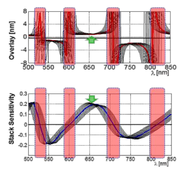 5.ACCURACY VERSUS CONSISTENCYTo verify the consistency of an overlay measurement, one could use a tool of reference. The SEM is very well positioned as it combines reasonable speed (even if slower than IBO and DBO tools) with in device measurements capability. The high voltage SEM is necessary to measure overlay when 2 layers are not on the same plan. The figure 17 demonstrates the need to go above 20 kVolts to ensure the visibility of the bottom layer and a good signal. Figure 17.Images of device versus beam voltage to enable the detection of the bottom layer in view of overlay measurements.  In table 3, the performance achieved on a BEOL process Metal 1 Litho-Etch-Litho-Etch process are comparable with standard performance of IBO or DBO in equivalent process. SEM overlay can be at minima a calibration tool to minimize the offsets with device. Table 3.Performance of different target design using High Voltage SEM on overlay targets [7]. Another traditional way of verifying the consistency is to compare measurements of the same target after lithography and after etch. It has to be noted that after_litho/after_etch consistency does not resolve the issue if the bottom grating is deformed as shown in chapter 3. The figure 18 combines after_litho/after_etch consistency check and the tool of reference being the SEM here. Grid correctables are compared using different methods: DBO after lithography, DBO after etch, SEM after etch. A difference of 0.5 to 1.5 nm can be observed between lithography and etch or compared to reference. If overall the agreement with the tool of reference is good, this last nanometer difference is so small that it is hazardous to pretend that one technique is more true than another. Figure 18.Grid correctables compared between DBO target after lithography and after etch to SEM measurements of the equivalent parameter.  In this chapter, we have shown that comparison of IBO/DBO to tool of reference, or through process consistency of overlay values can demonstrate a good agreement up to roughly 1 nm. Inaccuracy of several nanometers can be solved. But, beyond this nanometer, we are reaching the limits of resolution of the tool of reference. We do not know who is right and it is possible that this last nanometer inconsistency might not be resolved. Ultimately, electrical performance or yield is the only parameter that matters. As the last nanometer determination does not seem reachable today, the main focus must remain on robustness to ensure consistency (wafer to wafer, lot to lot). In other words, ensuring that any deviation from nominal is precisely detected, is more important for process control than accurate numbers. 6.THE IMPORTANCE OF SAMPLINGProcess control quality depends upon the quality as previously discussed but also the quantity of information received. To illustrate this point, the figure 19 shows that a high order model correction like CPE requires a very dense amount of information (by definition few points per field for all fields). Another case, already shown in the figure 12 is edge effect or intrafield fingerprints which require dense sampling. Figure 19.Dense sampling measured after litho. Raw data (right), residual fingerprint after 10 linear parameters removed (middle), residual fingerprint after Correction Per Exposure (CPE) model removed (right).  The figure 20 shows the impact of registration error inside a mask. Mask fingerprint can be a significant contributor. Characterizing Mask Pattern Placement Error [PPE] can be corrected based on wafer data [23]. But remaining fingerprints might need further characterization to enable high order intrafield correction. These sampling strategy of correction require a high speed of measurements that can be enable by the tool speed, but multi-layer target (Blossom, MLAIMid) can increase the measurement speed and extract more information [25]. 7.CONCLUSIONTable 4 below is a modified version of table 2 where we added the current status of these methodology. IBO is still heavily used. Beyond tool improvement the multi-patterning target is an enabler for complex control schemes. DBO is still the TMU champion but suffers of similar process issues than IBO. Finally SEM targets are showing very good performance and demonstrated to be capable of resolving significant offsets between IBO/DBO and design. Table 4.Summary of advantages and disadvantages of overlay target type landscapes. New complementary reference (High Voltage SEM) to calibrate optical techniques have been shown but there is no universal technique that combines all the advantages (speed, robustness, performance). Process effects are dominating, so consistency matters more than offsets or performance. Accuracy is nice to have; but not possible at last nanometer level. In consequence, target design optimization is key (segmentation, dummies, etc….) and simulation is mandatory with process knowledge and metrology limits. We have also shown that more and more wavelengths are needed to ensure target process robustness. In addition to the on wafer consistency, tool suppliers must ensure tool consistency provide machine internal tests to track hardware variations. Overlay metrology is a compromise between Real estate, MAM time and performance (Repeatability, Robustness and Accuracy). ACKNOWLEDGEMENTMircea Dusa from ASML; David Laidler from imec and Kit Ausschnitt for useful conversation and feedback. REFERENCESBenjamin Bunday,
“HVM Metrology Challenges towards the 5 nm Node,”
in Proc. of SPIE,
97780E-33 Google Scholar
Yoann Blancquaert,
“Diffraction Based Overlay and Image Based Overlay on production flow for advanced technology node.,”
in Proc. of SPIE,
86812O-2 Google Scholar
Mike Adel,
“Diffraction order control in overlay metrology: a review of the roadmap options,”
in Proc. SPIE,
(2008). Google Scholar
W. Yang,
“A Novel Diffraction Based Spectroscopic Method for Overlay Metrology,”
in Proc. SPIE,
200
–207
(2003). Google Scholar
H. –T. Huang,
“Scatterometry-based overlay metrology,”
in Proc. SPIE,
126
–137
(2003). Google Scholar
Philippe Leray,
“Achieving Optimum Diffraction Based Overlay Performance,”
in Proc. of SPIE,
76381 Google Scholar
O Inoue,
“SEM based overlay measurement between resist and buried patterns,”
in Proc. SPIE,
97781D
(2016). Google Scholar
Philippe Leray,
“Comparison of pattern placement errors as measured using traditional overlay targets and design rule structures.,”
in Proc. SPIE.,
49
(2003). Google Scholar
Jens T. Neumann,
“Overlay metrology for low-k1: challenges and solutions.,”
8326 832602
(2012). Google Scholar
A. Starikov,
“Accuracy of overlay measurements : tool and mark asymmetry effects,”
Opt. Eng., 31
(6), 1298
–1310
(1992). https://doi.org/10.1117/12.56172 Google Scholar
David Laidler,
“Identifying sources of overlay error in FinFET technology.,”
in Proc. SPIE.,
80
(2005). Google Scholar
Koen D’havé,
“Modeling for field-to-field overlay error.,”
in Proc. SPIE.,
83260U
(2012). Google Scholar
Hiro Tanaka1,
“Onset of Wiggling in a Microscopic Patterned Structure Induced by Intrinsic Stress During the Dry Etching Process,”
J. Appl. Mech, 81
(9), 091009
(2014). https://doi.org/10.1115/1.4027914 Google Scholar
Stephen Hsu,
“Overlay target design characterization and optimization for tungsten CMP.,”
in Proc. SPIE.,
360
(1998). Google Scholar
Igor Jekauc,
“Necessary nonzero lithography overlay correctables for improved device performance for 110nm generation and lower geometries.,”
in Proc. SPIE.,
228
(2004). Google Scholar
Peter Dirksen,
“Effect of processing on the overlay performance of a wafer stepper.,”
in Proc. SPIE.,
102
(1997). Google Scholar
Myungjun Lee,
“Metrology target design (MTD) solution for diagonally orientated DRAM layer,”
in Proc. SPIE,
97782R
(2016). Google Scholar
Martyn Coogans,
“The holistic approach to meet today’s patterning challenges,”
SEMICON TAIWAN,
(2015). Google Scholar
Jianming Zhou,
“Eliminating the offset between overlay metrology and device patterns using computational metrology target design,”
in Proc. Of SPIE,
97781G Google Scholar
Daniel Kandel,
“Overlay accuracy fundamentals.,”
in Proc. SPIE.,
832417
(2012). Google Scholar
K. Bhattacharyya,
“A study of swing-curve physics in diffraction-based overlay,”
in Proc. SPIE,
97781I
(2016). Google Scholar
Barak Bringoltz,
“Accuracy in optical overlay metrology,”
in Proc. SPIE,
97781H
(2016). Google Scholar
Philippe Leray,
“Compensating process non-uniformity to improve wafer overlay by RegC.,”
in Proc. SPIE,
905015
(2014). Google Scholar
W. Chou1,
“Mask Contribution to Intra-Field Wafer Overlay,”
in Proc. of SPIE,
–90501Q-4 Google Scholar
C. P. Ausschnitt,
“Multi-layer overlay metrology.,”
in Proc. SPIE.,
615210
(2006). Google Scholar
Philippe Leray,
“Diffraction based overlay metrology: accuracy and performance on front end stack.,”
in Proc. SPIE,
69220O
(2008). Google Scholar
Chih-Ming Ke,
“Accuracy of diffraction-based and image-based overlay.,”
in Proc. SPIE,
79711E
(2011). Google Scholar
Nuriel Amir,
“Multi layer overlay measurement recent developments.,”
in Proc. SPIE,
86812V
(2013). Google Scholar
|