

|
|
1.INTRODUCTIONIt is often said, and widely believed, that hands-on learning is the most effective and long-lasting approach to developing the deep knowledge and skills necessary to succeed in both industry and academic research environments. Foothill College has developed an effective microscopy concentration within a nanoscience and materials engineering program that includes training on a tabletop Scanning Electron Microscope (SEM) and Atomic Force Microscope (AFM) at Foothill, and access to Field Emission (FE-SEM) and Transmission Electron Microscopy (TEM) at NASA Ames Research Center (ARC) in the University of California Santa Cruz / NASA-Ames Research Center Advanced Studies Laboratories (“NASA-ASL”).[1] Foothill provides basic instrument training, including an introduction to microscopy, vacuum systems, data acquisition and image analysis. Students study materials and devices relevant in nanotechnology, and additionally use microscopy to support investigations in materials engineering. After gaining confidence and competence with these tools, students have an opportunity to learn to use a FE-SEM and TEM at NASA-ASL in the UCSC MACS (Materials Analysis for Collaborative Science) Facility at NASA Ames. Training at MACS is provided by a skilled and seasoned operator, providing instrument and advanced microscopy training. Students at NASA-ASL are treated as ‘interns’ and work with other research groups, as well as small business innovators, providing characterization skills, and in return learn about and participate in materials research and engineering, some of it in a very real-world context of product development. The problems we are addressing with this program are threefold. First, a study by SRI and Boeing in 2006 [2] determined that many engineering graduates with four-year degrees didn’t have the relevant experience, including Design of Experiments (DOE), analysis of data, and reporting results with conclusions and recommendations for follow on work. Recommendations from this study included having real world problems, scenario based curriculum, and access to industry relevant tools and instrumentation. This is a tall order for resource constrained community colleges, and easier said than done with respect to curriculum development. The second problem is access to internships, especially for community college students, who lack the skills to the ‘first pick’ of prestigious firms. Community college faculty often lack the time to build and sustain partnerships and relationships with industry. The third problem we address is the attrition of community college students and undergraduates in engineering programs, both from academic underpreparedness, as well as the social and academic maturity required to navigate and persevere through the challenges of increasingly longer college tenure. Added to this is the problem of industry that needs to provide extensive training to new hires before they can begin to become productive. An additional related problem is the lack of skilled workers to join start-up environments, work independently with some guidance, and learn quickly in at a development pace. A solution to all these problems is a program developed by Foothill College and NASA-ASL, where students, who show good academic promise, responsible work habits, and a commitment to longer term studies, learn to operate the FE-SEM and TEM. Training comprises three to five two hour guided sessions, and students train in pairs for cost efficiency. Instruments are available through an affordable cost recovery 'recharge' rate, allowing us to train ten to fifteen students a year. Samples include materials from real-world projects as well as small business entrepreneurs who also work in the collaboratory space. Small business gets access to otherwise price prohibitive tools, and in turn train students in applying characterization tools and analysis to engineering experiments and product development. Students not only get the type of experience they’d gain in a formal internship, they benefit from the dynamic and 'social' experience of working with a number of groups, including students more experienced and able to provide both technical as well as academic guidance. In a process we have named ‘socialization of science’, community college students gain from the guidance and maturity of older undergraduates and graduates, a process that occurs in universities in graduate and post doctorial programs, but in an informal process at ASL. In the year and a half that we have practiced this training program, students have found opportunities for employment in the small innovator companies at ASL, been hired by commercial laboratories, have found jobs after being laid off, and have transferred to four-year colleges and graduate programs, all as a result of the supportive and effective training and 'social mentoring'. The characterization emphasis in Foothill's nanoscience program follows a pedagogy funded by the National Science Foundation that integrates fabrication, characterization, and design of solutions for novel applications, where students learn the integrated approach of characterization of structures, process development, and process => structure => properties optimization. [3] The microscopy lab at Foothill is central to the materials characterization curriculum that also includes surface and elemental analysis. Students use the AFM to understand surfaces, metrology, and integration of AFM with SEM imaging. More advanced students use the FE-SEM / TEM to investigate nanostructures, including thin films, nanocarbon, and nanoparticle. Incubating innovation (I2), a novel NASA-ASL program that supports students at NASA, SJSU, and UCSC, blends materials engineering professionals with teams of students who flexibly provide and practice characterization skills to these entrepreneurial projects. Incubating Innovation (I2) is central to the intersection of two programs, informal education in STEM, and socialization of science, which bring together dozens of students from community colleges, undergraduate and graduate programs, and post doctoral programs. Students, staff, and faculty participate in collaborative research in the MACS Facility, sharing students with skills in microscopy and fabrication, and access to instruments made available through affordable recharge rates. This program facilitates group problem solving, critical thinking, and collaboration, skills sought in the workplace. It exposes students to dozens of research projects over the course of a year, where they choose two or three to be most involved with, but still 'collegially involved' with the scientific and research approaches to problems in advanced materials, including biomaterials, biomedical devices, and nanocarbon materials, using FE-SEM, TEM, and PE-CVD (Plasma-enhanced Chemical Vapor Deposition) process tools. The key to success of this program has been providing three tiers of instruments, Tabletop SEM, AFM, and FE-SEM and TEM, to three tiers of students; high school, community college, and undergraduate and graduate. Foothill College faculty will typically train high school and community college students on the tabletop SEM, and undergraduate and graduate students on the AFM. ASL staff and research faculty train students on the more advanced characterization and fabrications tools. The ASL environment fosters collaboration through the informally structured network of scientists, entrepreneurs, faculty researchers, and students, where the ‘socialization of science’ includes sharing the struggles, approaches, and insights of people with varied skills and academic maturity, and collaborative access to characterization and fabrication tools, which simulates the workplace environment. After a year and a half running the program, we have had a number of successes that we hope will become repeatable. These include placement of an intern at a commercial analytical laboratory after only five months in the program, based on 'polishing' of her resume and skills with the latest FE-SEM and TEM equipment, and real-world experience characterizing a number of novel materials, and hands-on operation of thin film processing tools. The dynamic nature of the collaboratory allows for 'easy on and easy off' fast skilling with sophisticated instruments, as well as experience working with real engineering problems. This is beneficial to technology veterans who become displaced in cyclical industry downturns, allowing them to build and regain their workplace confidence in a safe and supportive academic and research facility. A second intern, working with an entrepreneur for a number of months, became 'employee one' in the start-up, with flexible hours that allow him to stay in school and finish an undergraduate degree, while also mentoring our newer community college students. This student also participates in a novel outreach program to increase participation of engineering students from underserved communities and populations. 2.INTEGRATING MICROSCOPY INTO A MATERIALS ENGINEERING PROGRAMThe nanoscience and materials engineering program at Foothill College has utilized microscopy tools for almost a decade, beginning with the acquisition of an Atomic Force Microscope capable of running in contact and non-contact mode, providing demonstrations for students in metrology, and measuring surface topography on metals, ceramics, glasses, polymers, and thin films. This tool has also provided research grade images for graduate students at SJSU, and for some of our small business entrepreneurs in the collaboratory. In a recent NANO Camp at Foothill College, two high school students were able to operate the instrument (with guidance) in contact mode. Our more skilled students have also learned how to acquire images in non-contact mode, providing images of polymers as part of an engineering experiment (ref). Two years ago we purchased a new Hitachi TM-3000 Tabletop SEM, chosen for ease of use as well as durability. Every student who enters the nanoscience program at Foothill College will receive a demonstration of the AFM, and hands-on operation of the Tabletop SEM. For many students this is their first experience operating an instrument of any kind, and we spend time talking about and practicing good habits for sample preparation, mounting samples and proper pump down, and how to prepare and image non-conductive samples. Included in all training are safe laboratory habits, personal protective equipment, and proper operation and care of instruments. Students will appreciate these instruments are expensive to purchase and fix, especially for non-existent academic budgets for maintenance and repair. In addition to training as part of the coursework, we also provide an open laboratory on weekends for students in STEM related courses, as well as the community at large. We often have junior high school students operating the SEM with their parents, inspiring students to consider materials engineering as a course of study. Just as often, AP students from local high schools will approach us to use either or both the AFM and SEM on a materials related project, especially imaging biological artifacts. Beginning in fall 2014, Foothill College will teach a college level course through a local high school (PAUSD) and expect to have 20 to 30 students operating the SEM throughout fall in afternoons and on the weekends. These students will also learn about how each instrument operates, from the basic physics to the information that images and spectra provide, what types of materials can be analyzed, who uses these instruments (industries) to solve what types of problems (FA, QA/QC, materials characterization, etc). Materials engineering courses also tour the microscopy lab and learn to use the instruments, some applying them to their course work and projects. Examples of applications of these instruments include metal deformation, fatigue and failure, grain boundary engineering, metal finishing, corrosion analysis, particle size analysis, and some aspects of thin film engineering. Additionally, students will get an introduction to failure analysis, QA/QC, materials characterization, and process development, all different approaches to using microscopy tools in the context of research and development, manufacturing, and process engineering and control. These experiences and skills development help both students in an academic program, CTE (Career Technical Education), and incumbent worker training. Typical activities in the ASL laboratory include sputtering thin films and characterizing layer thickness, characterization of the graphitic nature of novel nanocarbon structures, including graphene, vertical graphene, and carbon nanospheres. Students learn to use a microtome, and other sample preparation tools. Students learn the principles behind physical and chemical vapor deposition, with applications for industry. Some industrial applications have included the deposition and characterization of metal/alloy nanolayers for solder joint forming materials. Furthermore, the opportunity to work on these industrial projects has also allowed interaction and mentorship from researchers and engineers from industry. 3.FIGURES AND EXPERIMENTSThree activities are illustrated with images showing the importance of microscopy in the nanomaterials and materials engineering program include preparation of gold nanoparticles and characterization with TEM, Focused Ion Beam preparation of samples for TEM, and use of FE-SEM in grain boundary engineering. Additionally, the Atomic Force Microscope was used to characterize a novel block co-polymer. Gold nanoparticles were synthesized from a solution of auric chloride using sodium citrate as a reducing agent. (In a similar approach we will also use silver nitrate and sodium citrate to make silver nanoparticles. The auric chloride solution is brought to a boil, after which a measured aliquot of sodium citrate was added. The solution was kept at a boil for ~15 minutes, during which time the solution turned deep ruby red. After cooling, a drop of solution was suspended on the TEM grid, from which the image in Figure 1 was obtained. Focused Ion Beam sample preparation is needed for a large fraction of samples analyzed by TEM. Additionally, TEM experience provides sample characterization for semiconductors, layered thin films, and nanostructured materials. One of the successful students who completed the program, Yessica Torres, operates a TEM and serves as a mentor to another Foothill College student, Anh Nguyen (See Figure 2) Figure. 2Foothill College student Anh Nguyen (left) mentored by TEM microscopist Yessica Torres (right). 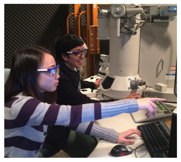 The Atomic Force Microscope was used to capture images of a block copolymer using close contact mode. Images of the surface from 5u x 5u (or 10u x 10u) scanned. (Figure 3). The AFM measurements showed unexpected step-edges of the material, which aided process development. These images provide insights into the unique molecular blending of the block co-polymers, as well as direction for future investigations. The Atomic Force Microscope was also used to capture images of a material showing step-edge (Figure 4) of a thin film of MnGaN. [4] These films were prepared using molecular beam epitaxy (MBE) of which the clip to hold the sample fortuitously provided an obstruction that varied the flux of Ga and N from the MBE source. [5] The Ga-limited growth conditions allowed for an increased amount of Group V species diffuse on the surface, thereby created a step-and-terrace formation. [6] The value of the microscopy training especially when used to support process development of sputtering, PE-CVD, nanocarbon synthesis and novel block co-polymers, is clear. Students combine characterization with processing to help determine structure => properties relationships, as well as how a particular processing path leads to a specific structure. From these two approaches (process => structure and stricture => properties) an integrated approach to materials engineering is developed (PNPC Rubric NSF-ATE 0903316 Final Report). This approach was found to be critical in developing technicians and professional engineer’s methodology in advanced materials engineering. It is especially important in small start-up environments, where there typically aren’t a large number of people in the company, and much of the development falls on one or two scientists, engineers, and or technicians. The ability to work in teams is especially important, which is a key element of the NASA-ASL collaboratory. Being able to bring in younger students with little instrument experience, beginning on a tabletop SEM and AFM, into a dynamic research environment, where they are supported by students of all levels provides an internship like opportunity, especially with opportunities to work with entrepreneurs with small scale development projects. Microscopes and image characterization are also critical in learning about materials, especially for chemistry and physics students, who often have no real formal experience with materials classification. Additionally, the use of image characterization is pivotal to developing an integrated approach to materials engineering, using structure => properties and processing => properties. This methodology has also received positive feedback from our industry advisory committee. 4.SUMMARY AND CONCLUSIONSThe availability of advanced microscopy tools at NASA-ASL is a somewhat unique opportunity that provides a learning environment which blends a supportive academic research effort with small technology entrepreneurs and the opportunity for students to use characterization tools in the context of real process develop. The cost of training is affordable, and has been successful in helping students obtain employment in brand name characterization facilities, as well as small start-up firms. Easy to use microscopy tools in a community college serve as a foundation for students to migrate into the research environment, an as importantly, provide an introduction to using both easy to use and research grade instruments as part of formal education in materials analysis. As importantly, having tools like a tabletop SEM that students from junior high school to high school can immediately use, provides a means to introduce students to STEM (Science Technology Engineering and Mathematics) in a safe, informal, and fun environment. Integrating microscopy into nanoscience and materials engineering is straightforward, and provides support for learning fundamental structure => properties relationships, using characterization tools to support R&D and process development, and provides technical tools for students conducting innovative research as part of their academic training and preparing for career development. REFERENCESUnpublished, SRI/Boeing internal document, Google Scholar
Cormia, R.D.,
“Advanced Technology Scenario Based Nanotechnicial Training,”
National Science Foundation Grant 0903316, Google Scholar
Ngo-Duc, T.T., Gacusan, J., Kobayashi, N.P., Sanghadasa, M., Meyyappan, M., Oye, M.M.,
“Controlled growth of vertical ZnO nanowires on copper substrate,”
Appl. Phys. Lett., 102 083105
(2013). https://doi.org/10.1063/1.4793758 Google Scholar
Shi, M., Chinchore, A, Wang, K.K., Mandru, A.O., Liu, Y.H., Smith, A.R.,
“Formation of manganese delta-doped atomic layer in wurtize GaN,”
J. Appl. Phys., 112 053517
(2012). https://doi.org/10.1063/1.4750034 Google Scholar
Ngo-Duc, T.T., Gacusan, J., Kobayashi, N.P., Sanghadasa, M., Meyyappan, M., Oye, M.M.,
“Controlled growth of vertical ZnO nanowires on copper substrate,”
Appl. Phys. Lett., 102 083105
(2013). https://doi.org/10.1063/1.4793758 Google Scholar
Oye, M.M., Shahrjerdi, D., Ok, I., Hurst, J.B., Lewis, S.D., Dey, S., Kelly, D.Q., Joshi, S., Mattord, T.J., Yu, X., Wistey, M.A., Harris, J.S., Holmes, A.L., Lee, J.C., Banerjee, S.K.,
“Molecular-beam epitaxy growth of device-compatible GaAs on silicon substrates with thin (similar to 80 nm) Si1-xGex step-graded buffer layers for high-kappa III-V metal-oxide-semiconductor field effect transistor applications,”
J. Vac. Sci. Technol. B, 25 1098
(2007). https://doi.org/10.1116/1.2713119 Google Scholar
|


